Building a Nios V soft processor system on the Agilex 3 dev kit
 Altera Agilex 3 FPGA and SoC C-Series Development Kit
We are living in the AI era, this is true and everybody knows it, but today we are living through another revolution in the world of processor design: the rise of RISC-V processors and also soft-cores.
This year’s DEFCON badge was based on an ASIC that, inside, had a Vexriscv core, a popular open-source RISC-V soft processor. Very big companies like Microchip are integrating RISC-V cores (hard) into their chips as well, and even though other vendors like Altera and AMD still use ARM cores for their hard processors, both already have RISC-V versions of their soft-cores, MicroblazeV and the one that will be the main character of this article, the Nios V.
But before Nios V, there was another soft-core from Altera (actually two). The first one was the original Nios, released in 2000 (one year before Microblaze). This core uses a RISC architecture with 16-bit instructions. Then, 3 years later, Altera presented Nios II, which improved performance and added more features, like a 32-bit architecture and three different flavours: economy, standard and fast, and it stayed alive until 2023. Two years before that, Nios V arrived. It is based on the RISC-V architecture and also comes in three different flavours: Compact, with basic functionalities; Microcontroller, with complete features for embedded development; and General Purpose, which is the high performance option.
In this article we are going to take a look at the Nios V processor, how to integrate it into the Agilex 3 fabric using Platform Designer, and how to build and run a simple application on it. SPOILER: it is surprisingly straightforward to create applications for it from the command line.
Everything here is done with Quartus Prime Pro 26.1.1 on the Agilex 3 FPGA and SoC C-Series Development Kit, device A3CW135BM16AE6S. The complete project, system description and application included, is in the GitHub repository under niosv/.
Table of contents
- Creating the project and the system
- The reset scheme
- Addresses, top level and pins
- Generating the BSP and the application
- Programming the board
- Conclusions
Creating the project and the system
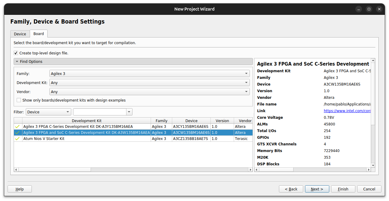
When Quartus asks which device the project targets, there is a tab most people walk straight past. Instead of picking the device out of the list, you can pick the development kit, and selecting the Agilex 3 FPGA and SoC C-Series Development Kit brings in the board definition together with the device.
Since the whole design is going to be built around a soft core, the next step is Platform Designer. The first time you open it in a new project it has nowhere to put the system description, so it asks where to create the .qsys file — I keep it in the project folder next to the .qpf, which matters later because both niosv-bsp and niosv-app take paths to those two files.
A new system always starts with a Clock Bridge IP and a Reset Bridge IP, and both need attention before anything else, because their defaults do not match this board (I honestly miss an automatic board configuration). The clock bridge is configured for 50 MHz and the board reference clock on pin AJ27 is 100 MHz, so that value has to be corrected, then it will be propagated to the rest of the IPs, so getting it wrong gives you a processor that reports the wrong frequency and every delay loop off by a factor of two. The reset bridge defaults to an active-high reset, and the pushbutton wired to it, io96_3a_pb1_fpga_rst_n, is active low. Checking Active low reset fixes it and, as a side effect, renames the exported port to reset_reset_n.
Choosing the Nios V flavour
As I mentioned before, Nios V comes in three variants, and the IP Catalog lists all of them under Processors and Peripherals > Embedded Processors:
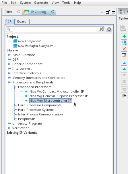
Nios V/c is the compact one, Nios V/g is the general purpose core, and Nios V/m is the middle option, a straightforward microcontroller architecture, and it is the one I use here — this system is a controller for fabric logic, not a general purpose computer, and the board already has a Cortex-A55 if I want Linux.
All the configuration options stay at their defaults except one: Enable Reset from Debug Module.
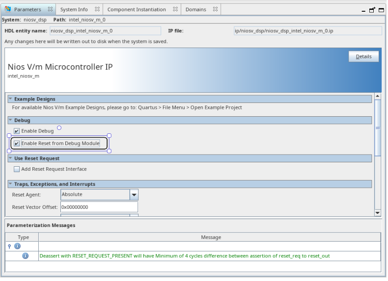
That option exposes the dbg_reset_out and ndm_reset_in ports, and without it the debugger cannot reset the processor. In practice that means every time you download a new build you have to walk over to the board and press the reset button, which gets old within about ten iterations.
The rest of the peripherals
A processor on its own does nothing, so the system also gets:
- On-Chip Memory II (RAM or ROM) IP, where the application lives.
- JTAG UART IP, which carries both the debugger connection and
stdout, soprintfends up on your terminal. - Reset Release IP, which provides the
ninit_donesignal. More on this in the next section — it is not optional. - SPI (4 Wire Serial) IP, an Avalon-attached SPI master brought out to the expansion header.
- PIO (Parallel I/O) IP, a simple GPIO block driving the two board LEDs.
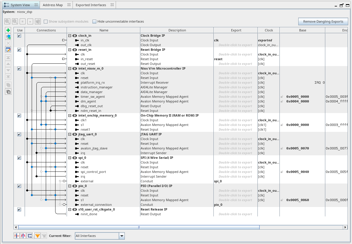
The connection rules are mechanical once you know them. Every peripheral the processor has to reach gets its s1 Avalon agent port connected to the processor’s data_manager port. All the clock inputs go to the clock bridge output. And anything that leaves the FPGA — the LED pins, the SPI signals — has to be exported, by double-clicking in the Export column, which is what makes it appear as a port on the generated top-level module.
The reset scheme
This is the part that decides whether the board comes up on its own after configuration, and it is worth more attention than it usually gets.
There are three separate reset sources in this system and each one has a rule.
The Reset Release IP produces ninit_done, which is the signal that says device configuration has finished. It has to go to the reset input of every component: the CPU, the on-chip memory, the PIO, the SPI and the JTAG UART. Leaving one peripheral out of that list is the classic failure — the system does not start after configuration and you have to press PB1 by hand to get it going.
The reset bridge, fed by the PB1 pushbutton through reset_in.out_reset, goes to the same five components. This is the manual reset, and as noted above the bridge must have Active low reset checked to match the board.
The third one is the important one for debugging. The debug module’s dbg_reset_out must be connected to ndm_reset_in, and never to the CPU’s reset port. This is not a style preference, the Nios V handbook forbids it explicitly:
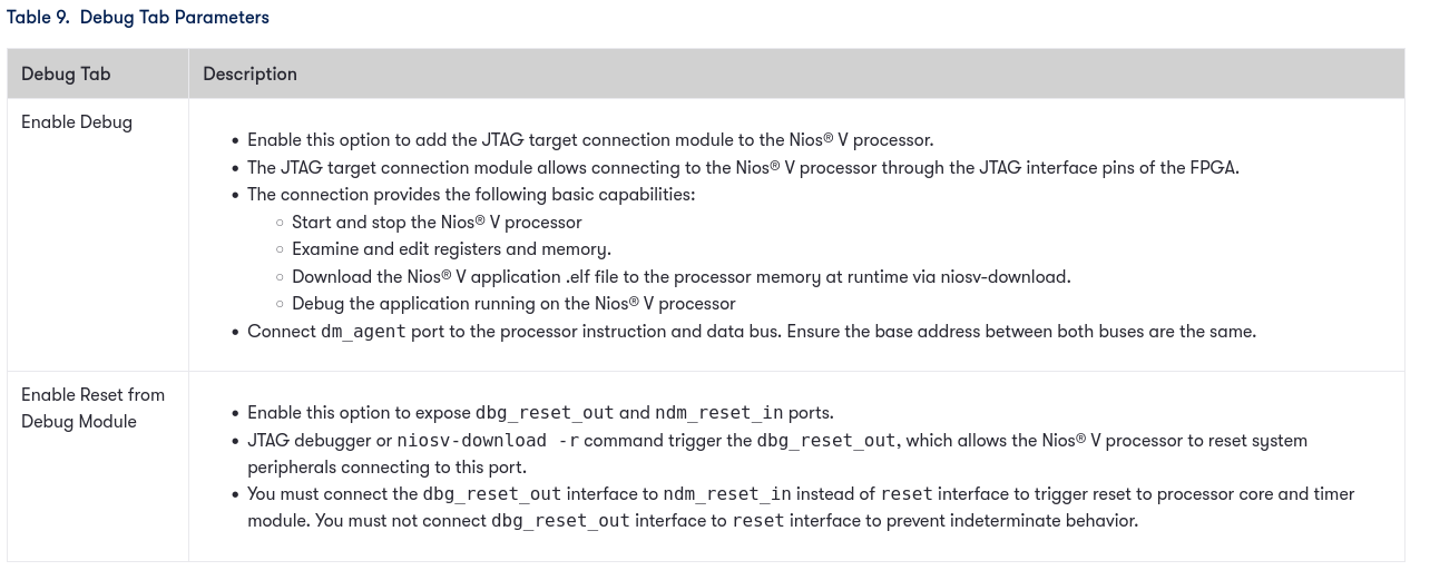
Wire it to reset and the debug module ends up resetting itself. The symptom is specific enough to be worth writing down: the first niosv-download after configuring the FPGA works perfectly, and every subsequent one fails with Could not halt the target. If you are chasing that error, this is where to look before anything else.
Addresses, top level and pins
With everything connected, the Address Map tab is where each Avalon agent gets its slot. Unlike the golden reference design of the previous articles, this system is mine from scratch, so there are no existing addresses to preserve and letting the tool assign them is perfectly safe. The result for this design puts the on-chip memory at 0x0000_0000, and the peripherals up at 0x0005_0040 for the SPI, 0x0005_0060 for the PIO and 0x0005_0070 for the JTAG UART.
Those numbers matter because they come back as #defines in the generated system.h, and that is how the application addresses them — you never type an address in the C code.
After that it is Verify System, Generate HDL, and setting niosv_dsp as the top-level entity of the Quartus project. Running Analysis and Elaboration then gives Quartus a netlist with real port names, which is the precondition for the Pin Planner to be useful.
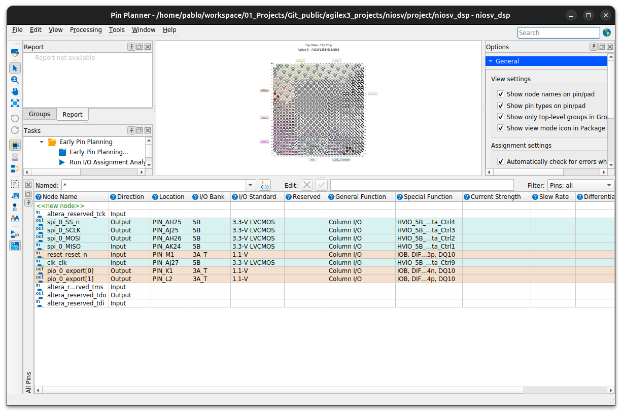
The assignments for this design are the 100 MHz reference clock clk_clk on AJ27, the pushbutton reset_reset_n on M1, the two LEDs pio_0_export[0] and [1] on K1 and L2, and the four SPI signals on bank 5B. Note that the LEDs and the pushbutton sit in bank 3A at 1.1 V while the clock and the SPI pins are 3.3-V LVCMOS in bank 5B — the banks on this board are not all at the same voltage, and the Pin Planner will tell you about it only after you assign something incompatible.
One step that is easy to skip: run Processing > Start I/O Assignment Analysis. The JTAG pins (altera_reserved_tck, tms, tdo, tdi) are dedicated SDM pins rather than user I/O, so you do not assign them by hand — this analysis fills them in and verifies the rest of the assignments are legal before you commit to a full compilation.
The timing constraints for this system are short, because most of it does not need constraining. There is one real clock, the pushbutton is asynchronous and resynchronised inside the reset controller, and nothing samples the LEDs:
set clk_period 10.000
create_clock -name {clk_clk} -period $clk_period [get_ports {clk_clk}]

set_false_path -from [get_ports {reset_reset_n}]
set_false_path -to [get_ports {pio_0_export[*]}]
The SPI pins are cut with false paths too, but only because no slave is wired to them yet. The moment a real device hangs off that header those have to be replaced with proper source-synchronous constraints referenced to the generated SCLK clock that the SPI IP creates, using the tsu/th/tco figures from the slave’s datasheet.
Generating the BSP and the application
Here is where I leave the GUI behind. The board support package is generated from the .qsys description with niosv-bsp:
cd software
mkdir -p blink

niosv-bsp -c -t=hal \
  -s=../project/niosv_dsp.qsys \
  -p=../project/niosv_dsp.qpf \
  bsp/settings.bsp
-t=hal asks for the hardware abstraction layer BSP rather than a bare-metal one, and the result is a bsp/ folder containing the drivers for the IPs in the system, a linker script, and the system.h with all the addresses and parameters baked in from the hardware.
The application itself is deliberately trivial — the point is to prove the whole chain works, not to write firmware:
#include <stdio.h>
#include "system.h"
#include "altera_avalon_pio_regs.h"

int main(void) {
  unsigned int i = 0;

  printf("Hello from NiosV running at %d Hz\n", (int)ALT_CPU_FREQ);

  while (1) {
    IOWR_ALTERA_AVALON_PIO_DATA(PIO_0_BASE, i & 0x3);
    i++;
    for (volatile int d = 0; d < 1000000; d++);
  }

  return 0;
}
Note that neither the LED address nor the clock frequency is written by hand: PIO_0_BASE and ALT_CPU_FREQ come from system.h, which came from the .qsys. Change the base address in Platform Designer, regenerate the BSP, and the software follows without an edit. The printf goes out over the JTAG UART.
Turning that into a buildable project is one more command, which writes a CMakeLists.txt wiring the application against the BSP:
niosv-app -a=blink -b=bsp -s=blink/main.c

cmake -S blink -B blink/build -G "Unix Makefiles"
make -C blink/build
The compiler that gets picked up is the RiscFree toolchain that ships with Quartus, riscv32-unknown-elf-gcc, GCC 15.2.0 in this release. It is a standard RISC-V bare-metal toolchain, which is one of the nicer consequences of Nios V being RISC-V rather than the proprietary ISA that Nios II used.
When the linker runs out of memory
The first make did not get that far:
./../../riscv32-unknown-elf/bin/ld: region `intel_onchip_memory_0' overflowed by 43256 bytes
collect2: error: ld returned 1 exit status
This is a good error to hit early, because it makes the relationship between the hardware and the software concrete. The linker script in the BSP describes a memory region whose size came from how I configured the On-Chip Memory IP — 64 KB — and the application does not fit in it. What I did next was increase the size of the on-chip memory in Platform Designer.
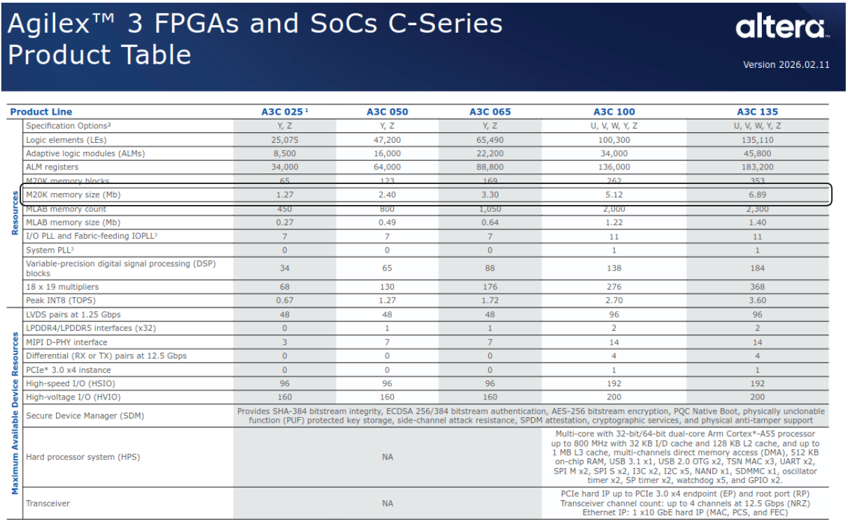
I raised it to 256 KB, comfortably more than the ~107 KB the link actually needed, since this device has 6.89 Mb of embedded memory in total and there is no reason to be frugal at this stage. What is easy to forget is that changing the size changes the address map, so the base addresses have to be reassigned and the HDL regenerated — and then the whole software side has to be regenerated too, because system.h and the linker script are both derived from the hardware:
niosv-bsp -c -t=hal -s=../project/niosv_dsp.qsys -p=../project/niosv_dsp.qpf bsp/settings.bsp
niosv-app -a=blink -b=bsp -s=blink/main.c
cmake -S blink -B blink/build -G "Unix Makefiles"
make -C blink/build
That sequence is the reason I do this from the command line instead of the IDE. It is four commands that always run in the same order after any hardware change, which makes it a script rather than a sequence of dialogs to click through.
With the link succeeding, the build directory has what we need:
$ ls blink/build
blink.elf  blink.elf.objdump  bsp  CMakeCache.txt  CMakeFiles
cmake_install.cmake  intel_onchip_memory_0.hex  Makefile
The .hex is the memory initialisation file, which would let you bake the application into the bitstream. For the development loop we want the .elf instead, downloaded over JTAG.
Programming the board
Two separate operations, in order: configure the FPGA with the hardware, then load the software into the processor that now exists inside it.
Before either, it is worth checking what the JTAG chain actually contains:
$ jtagconfig

1) AG3C_SoC_DK [1-1.4.2-iface0]
  4BA06477   ARM_CORESIGHT_SOC_600
  4369B0DD   A3C(W135BM16A|Y135BM16A)/..
We can see that tere are two devices on the chain. The first is the Arm CoreSight debug access port belonging to the hard processor system, the Cortex-A55 from the previous articles. The second is the FPGA. Since we are configuring the fabric, the device index we need is 2, and that is what the @2 suffix means here:
quartus_pgm -c 1 -m jtag -o "p;output_files/niosv_dsp.sof@2"
Then the application goes into the Nios V:
niosv-download -g -r ./blink/build/blink.elf
-g starts the processor after downloading and -r resets it first — and this is the step that silently depends on the reset scheme being right. If dbg_reset_out went to the wrong port, this is exactly where it works once and then never again.
At this point the LEDs start counting, and the greeting arrives over the JTAG UART with the frequency read straight from the hardware description.
Conclusions
I have always said that the real power of FPGA based SOCs comes from the ability to tailor both the hardware and the software to the specific needs of the application, rather than being constrained by a fixed architecture. There is something that I liked a lot about NiosV and Quartus, and it is that, once the hardware design is complete, you have all you need to build and run the corresponding software with different commands that can be scripted and automated, making the development process more efficient and reproducible, and also more AI friendly, you know.
Bare-metal is indeed an option, but using an operating system can provide additional abstractions and services that simplify development for more complex applications, and I am not talking just about Linux, but also other operating systems like Zephyr, and it is a path that I am exploring with NiosV for future projects.