Reconfiguring the Agilex 3 FPGA fabric from Linux without rebooting
 Altera Agilex 3 FPGA and SoC C-Series Development Kit
In the previous article we booted Linux on the Agilex 3 HPS and added a custom Avalon-MM peripheral, avalon_matrix_mult, to the fabric of the Golden System Reference Design. Now it’s time for Linux.
The design we built left us with a working accelerator and a very slow development loop: the documented path to get a new fabric onto the board is to rebuild the whole SD card image and power-cycle, for every single change. No way…
The idea of an SoC is that, having the FPGA directly connected to the processor, you should be able to reconfigure it on the fly without needing to reboot the entire system. This is exactly what the FPGA Manager and device tree overlays allow you to do in Linux. This time, we will see that there is no typical FPGA Manager that can be used with the fpgautil command, but it is not too different. What is different is the boot of the Agilex 3 (and 5 and 7), in comparison with other devices we have seen in the blog before.
Again, I needed the help of AI assistance to figure out the exact steps and pitfalls involved in reloading the FPGA fabric from Linux, especially because it is something that is not well documented for these parts. I guess they rely on the Yocto documentation for this.
Table of contents
- How this board boots
- What you can actually swap at runtime
- Loading the new fabric from Linux
- Testing the IP from userspace
- Conclusions
How this board boots
The starting point is understanding how this board actually boots, because that is what decides which changes you are allowed to make. The Agilex 3 SoC supports two boot modes, and the GSRD baseline uses HPS Boot First. That is not a detail to skim over: the Altera booting guide states that configuring the FPGA fabric from HPS software is supported only when using this mode. One point for Altera!
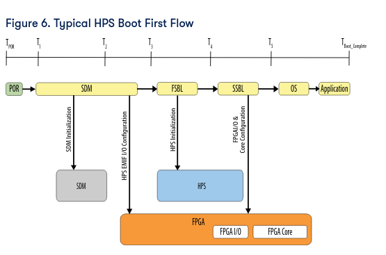
Read that left to right. The SDM initializes itself and configures the HPS EMIF I/O — this is phase 1, and on this board it comes from the ghrd.hps.jic programmed in QSPI. The FSBL then brings up the HPS. And it is the SSBL, U-Boot, that configures the FPGA I/O and the FPGA core — phase 2, which travels inside the kernel.itb on the SD card. Every pin allocated to the FPGA stays tri-stated until that last step completes.
What you can actually swap at runtime
Now, from the last article, we have the .sof file for the whole design. From this file, we can generate the .rbf file with quartus_pfg command:
quartus_pfg -c output_files/baseline.sof output_files/baseline_mm.core.rbf \
            -o hps=ON -o hps_core_only=ON
hps=ON tells the tool the design contains an HPS. hps_core_only=ON asks to separate the HPS and the FPGA, so the .rbf will be split into a periphery part and a core part.
Those two options are worth spelling out, because they are the whole reason the “do not touch the I/O” rule exists. This is what each half carries:
| File | Contents | Loaded by |
|---|---|---|
*.periph.rbf |
The FPGA I/O ring: pin locations, I/O standards, PLLs, transceivers | U-Boot at boot, from kernel.itb |
*.core.rbf |
The fabric logic itself, the CRAM contents | U-Boot at boot — or Linux at runtime |
When you reconfigure from Linux you give to the FPGA Manager a *.core.rbf and nothing else. The I/O ring that is configured in the device is still the one U-Boot programmed at boot, and no part of the file you are sending describes it. This is important, the bitstream you are giving it does not contain pins at all.
The command prints three hashes, and they are the most important output of the whole step:
IO hash     is E2271184D92C9A98774D7314AF6C7E80D616EDE75541DBAF4B3DE4C8EEEB7A60
HPS IO hash is 494A826195216B83ECA008B60BE6CDF017D192B42E53963B154953B2DCA8FAB5
Design hash is B3999BD833D90DBDFDFC2EDCCB390AAF31A2B4E33174010C585271C897DE27F9
There are exactly three of them because they map onto the three pieces of the puzzle, and the two you are not replacing are the two that have to match:
HPS IO hashcovers the HPS pin mux and the EMIF — phase 1, sitting in QSPI. The HPS is running on it right now, including the DDR your kernel lives in. It must match.IO hashcovers the FPGA I/O ring, configured by U-Boot as part of phase 2. You are not reloading it either. It must match.Design hashcovers the core, which is the only thing you are actually swapping. This one is free to change, and in practice it will. That difference is your new logic.
A word of warning on that last one: a different design hash is a useful confirmation that you built what you think you built, but it is not a requirement. Reloading a bitstream identical to the one already running is perfectly legal, and the SDM accepts it — I did it more than once while debugging.
The design compatibility section of the booting guide lists what feeds those hashes: I/O configuration, pin locations, PLLs and clock spine differences. In practice that gives a clean rule for what breaks a runtime reload. Editing the .qsf pin assignments, changing an I/O standard, adding a PLL or re-routing an HPS peripheral to different pins all move an I/O hash, and the reload will be rejected. Changing logic inside the fabric only moves the design hash, and that is precisely the case of avalon_matrix_mult.
This also gives you a cheap test that costs one command instead of a trip to the board: run quartus_pfg and compare the IO hash against the one from the unmodified golden design. If it changed, you have touched the periphery somewhere without meaning to, and no amount of retrying on the target will help.
What happens when they do not match is worth knowing, because it does not look like a rejection. In my experience the SDM accepts the command and then quietly stops consuming data partway through the transfer: no error code, no kernel message, just a write that never returns and an fpga0/state stuck at write. This is the real reason the whole design has to be built from the same GSRD revision and the same Quartus release that produced the SD card image — the booting guide is explicit that both files must come from the same Programming File Generator version so they carry the same SDM firmware version.
Loading the new fabric from Linux
To load the new design into the fabric, we need to copy the .rbf and a device tree overlay both go to /lib/firmware on the target, which is where the kernel firmware loader looks. The overlay and the scripts used in this article are in the GitHub repository under hps_custom_ip/linux/:
scp output_files/baseline_mm.core.rbf root@192.168.125.112:/lib/firmware/
scp hps_custom_ip/linux/matrix_mult_reload.dts root@192.168.125.112:/lib/firmware/

ssh root@192.168.125.112 'cd /lib/firmware && \
  dtc -@ -I dts -O dtb -o matrix_mult_reload.dtbo matrix_mult_reload.dts'
The overlay is tiny. All it does is point the FPGA region at the new bitstream:
/dts-v1/;
/plugin/;
/ {
    fragment@0 {
        target-path = "/fpga-region";
        __overlay__ {
            firmware-name = "baseline_mm.core.rbf";
            config-complete-timeout-us = <30000000>;
        };
    };
};
Check the node name against your own device tree before copying this. The Altera examples for Agilex 5 and Agilex 7 target /soc/base_fpga_region or /soc@0/base_fpga_region; this BSP exposes it as /fpga-region, and ls /proc/device-tree/ on the target settles it in one command.
Isolating the fabric first
This is the part that is missing from the documentation, and skipping it hangs the board.
The PIO peripherals of the golden design live inside the fabric, behind the LWH2F bridge, and Linux has drivers bound to them:
root@agilex3:~# cat /sys/kernel/debug/gpio
gpiochip2: 32 GPIOs, parent: platform/20010080.gpio, /soc@0/gpio@20010080:
 gpio-0   (                    |fpga_led0           ) out lo
 gpio-1   (                    |fpga_led1           ) out lo
 gpio-2   (                    |fpga_led2           ) out lo
gpiochip3: 32 GPIOs, parent: platform/20010060.gpio, /soc@0/gpio@20010060:
The moment the SDM starts rewriting the fabric, those registers stop answering. Any AXI transaction issued by a driver that is still bound never completes, the CPU stalls on it, and the watchdog resets the board. On my first attempt this looked like a random crash, with the kernel log flooded with one of these every 26 microseconds:
EDAC Altera: SEU UE: Count=0x8, SecAddr=0x10020, ErrData=0x100
That message is the CRAM scrubber noticing that the configuration RAM no longer matches its ECC — exactly what you would expect while the fabric is being rewritten underneath it.
Normally the kernel prevents all of this by itself: fpga_region_program_fpga() disables the bridges before programming. On this BSP it cannot, because there is nothing to disable:
root@agilex3:~# ls /sys/class/fpga_bridge/
root@agilex3:~#
The GSRD device tree declares an fpga-region and an fpga-mgr, but no fpga-bridge nodes, so the LWH2F stays wide open for the whole operation. Until that is fixed in the BSP, the drivers have to be unbound by hand:
echo "soc@0:leds"  > /sys/bus/platform/drivers/leds-gpio/unbind
echo 20010080.gpio > /sys/bus/platform/drivers/altera_gpio/unbind
echo 20010060.gpio > /sys/bus/platform/drivers/altera_gpio/unbind
It is also worth silencing the console and the scrubber (the block that is continuously looking for errors in the memory) before starting. A printk storm at 26 microsecond intervals into a 115200 baud serial console is its own way of wedging a system:
dmesg -n 1
echo 0 > /sys/devices/system/edac/cram-seu/log_ue
Applying the overlay
With the fabric isolated, the reconfiguration itself is two commands:
mkdir -p /sys/kernel/config/device-tree/overlays/reload
echo matrix_mult_reload.dtbo > /sys/kernel/config/device-tree/overlays/reload/path
The mkdir does not create a real directory. Configfs intercepts it and instantiates an overlay object in the kernel, with its own path, dtbo and status files. Writing the filename into path is what triggers everything: the kernel loads the .dtbo from /lib/firmware, sees that the target is an fpga-region node and hands over to the region driver, which reads firmware-name, loads the 1.6 MB .rbf and passes it to the FPGA Manager. The Stratix10 SOC FPGA Manager driver — Agilex 3 reuses it — then talks to the SDM through the Altera service layer, sending COMMAND_RECONFIG and streaming the bitstream in 512 KB buffers.
That write blocks until the operation finishes, roughly two seconds. If the SDM rejects the content it will sit there until the timeout expires, which is why it is worth running it detached with a guard instead of from an interactive shell.
Afterwards you check the result and bind the drivers back:
cat /sys/class/fpga_manager/fpga0/state      # operating
echo 20010060.gpio > /sys/bus/platform/drivers/altera_gpio/bind
echo 20010080.gpio > /sys/bus/platform/drivers/altera_gpio/bind
echo "soc@0:leds"  > /sys/bus/platform/drivers/leds-gpio/bind
The states you will see in fpga0/state are unknown before touching anything, write while the bitstream is being transferred, and operating when it completed. If it stays stuck in write, the SDM stopped consuming buffers — almost always an I/O hash mismatch.
All of this is wrapped in a small shell script on the target, so a full iteration is one command:
root@agilex3:~# ./fpga_reload.sh baseline_mm.core.rbf
== 1. lowering console verbosity and silencing SEU ==
== 2. isolating the fabric (unbinding LEDs and PIO) ==
   OK: fabric isolated
== 3. generating overlay ==
== 4. reconfiguring ==
   rc=0  fpga0=operating
== 5. rebinding fabric peripherals ==
   leds: fpga_led0 fpga_led1 fpga_led2 hps_led0 hps_led1
== RESULT: fpga0=operating  SEU_UE=0 ==
Testing the IP from userspace
The first thing to read is the identification register, which is the entire reason the IP has one:
root@agilex3:~# devmem2 0x20010400 w
/dev/mem opened.
Memory mapped at address 0xffff8b1f7000.
Read at address  0x20010400 (0xffff8b1f7400): 0x4D4D554C
Reading back MMUL in ASCII is conclusive: the fabric was rewritten while Linux kept running, and the new peripheral answers on the Avalon bus at the address assigned in Platform Designer.
From there a shell script exercises the whole register map — it loads both operand matrices, starts the engine, polls the status register and compares the result against a reference computed in the shell:
root@agilex3:~# ./matrix_mult_test.sh
avalon_matrix_mult @ 0x20010400

  ID     : 0x4D4D554C (MMUL, ok)
  SIZE   : 4 (4x4, 16 elements per matrix)

  A =
             1       2       3       4
             5       6       7       8
             9      10      11      12
            13      14      15      16
  B =
             2       1       1       1
             1       2       1       1
             1       1       2       1
             1       1       1       2

  done after 1 status poll(s), busy=0 done=1

  C (hardware) =
            11      12      13      14
            31      32      33      34
            51      52      53      54
            71      72      73      74

  ==== RESULT MATCHES THE REFERENCE ====
The script reads the matrix order from the SIZE register instead of assuming it, so rebuilding the IP with a different matrix_size needs no change in software. And one status poll is enough: the engine does one multiply-accumulate per clock cycle, so a 4x4 takes 64 cycles, around 0.64 microseconds at 100 MHz — long finished before devmem2 has even completed its mmap.
Conclusions
The experiment demonstrates that it is possible to reload the FPGA fabric on an Agilex 3 SoC without rebooting Linux, and that the new hardware can be immediately accessed from userspace. This opens the door to many different projects and also simplifies the development workflow, reducing the iteration time for hardware-software co-design.
The fact that you can’t modify the I/O pins without a full reboot is not actually a big limitation. Usually you will have a hardware design where the I/O configuration is stable, and the parts of the design that benefit from frequent updates are the internal logic blocks, which can be reloaded without affecting the I/O. Also, in the case of accelerators, they don’t use the I/O pins directly, so, although it could seem a limitation, it rarely impacts the practical use of reconfigurable logic.
If you need to know the boot process of these devices in depth, you should read the Hard Processor System Booting User Guide. It is dense, but it is very well explained and provides all the necessary details for understanding how the system initializes and loads the FPGA fabric.