CryptoliteICE: an Open-Source FPGA-Based TRNG
One of the missions of an engineer, is selects the device that fits better for a project. In the case of FPGA engineers, of even any embedded software engineer, many times we tend to use always the same devices because we feel comfortable with them, we have experience with them, the toolchain configured… But sometimes we a working in a project that, because of the requirements, the best option is a different device. In this post I will talk about CryptoliteICE, a FPGA-based True Random Number Generator that I built using an ICE40 FPGA and a RP2040 microcontroller. I will explain why I chose these devices, how I implemented the TRNG, and how to build and use it.
A True Random Number Generator sits at the foundation of almost every cryptographic system — key generation, nonces, IVs, session tokens — yet it rarely gets much attention in hardware projects. Software pseudo-random number generators work well enough for many scenarios, but when security actually matters you want entropy rooted in physical noise, not in a deterministic state machine that an attacker can predict if they recover the internal state.
CryptoliteICE is a small USB stick I built for the lut7.dev research initiative that solves this problem with two inexpensive off-the-shelf chips. A Lattice iCE40UP5K FPGA generates raw entropy from 32 parallel ring oscillators running concurrently; a Raspberry Pi RP2040 microcontroller reads that raw bitstream over SPI, runs NIST SP 800-90B continuous health tests, applies SHA-256 conditioning, and exposes the result as a USB Vendor device. The host side is a single Python script. The HDL, firmware and the board schematic are open source.
This post covers the design decisions, the ring oscillator implementation, the RP2040 conditioning pipeline, and how to build and use the device.
Table of contents
- Why an ICE40 FPGA?
- ICE40 FPGA implementation
- The RP2040 as platform controller
- From entropy to conditioned bytes
- The hardware
- Getting started
- Conclusions
Why an ICE40 FPGA?
I have written before about TRNGs on FPGAs and the core idea is the same: ring oscillators in programmable logic carry physical jitter you can harvest as entropy. The ICE40 family in particular is a good fit for this type of project for a few reasons.
Low cost. The iCE40UP5K-SG48ITR costs a few euros in small quantities, which keeps the BOM reasonable. For a project aimed at open sharing and reproduction, that matters.
Open-source toolchain. The ICE40 family is the one FPGA family with a complete open synthesis and place-and-route flow: yosys handles synthesis, nextpnr-ice40 does placement and routing, and icepack packs the bitstream. No licences, no annual subscriptions, no 20 GB installers, no license changes. The entire FPGA build fits into a shell script of about 30 lines with no proprietary dependencies — which is particularly important for a security component where you want to be able to inspect and reproduce every step.
SB_LUT4 primitives. Ring oscillators must survive synthesis without being optimised away or transformed into something that eliminates the jitter. On AMD FPGAs you use LUT1 with dont_touch attributes; on iCE40 you can instantiate SB_LUT4 directly as a black-box primitive that yosys treats as opaque, giving you precise control over the oscillator topology without relying on synthesis tool attributes.
Small package. The SG48 package — 6 × 6 mm QFN-48 — is compact enough to sit alongside an RP2040 on a USB-stick PCB with room to spare. 5 k LUTs is far more than necessary for the TRNG logic.
ICE40 FPGA implementation
The entropy source is a bank of ring oscillators built from SB_LUT4 primitives. A ring oscillator consists of an odd number of inverting stages in a closed loop: because the total inversion count is odd, the circuit cannot settle at a stable logic level and oscillates continuously. The oscillation frequency depends on the propagation delay through each stage, which is influenced by temperature, supply voltage noise, manufacturing variation, and thermal noise in the transistors. These physical effects introduce timing jitter that is the primary entropy source.
The ro_cell module implements one 8-stage ring oscillator: one SB_LUT4 configured as a buffer (which closes the ring feedback from the last stage back to the first) and seven SB_LUT4 stages configured as inverters. Seven inversions give an odd total, guaranteeing oscillation. The (* keep *) attribute prevents yosys from pruning the feedback wire, and using the SB_LUT4 primitive directly prevents the stages from being absorbed into a larger logic cone during synthesis:
module ro_cell (
  output wire out
);

  localparam N_STAGES = 8;

  (* keep *) wire [N_STAGES-1:0] chain;

  /* Stage 0 — buffer, closes the ring feedback */
  (* keep *) SB_LUT4 #(.LUT_INIT(16'hAAAA)) u_buf (
    .I0(chain[N_STAGES-1]),
    .I1(1'b0),
    .I2(1'b0),
    .I3(1'b0),
    .O(chain[0])
  );

  /* Stages 1–7 — inverters */
  genvar j;
  generate
    for (j = 1; j < N_STAGES; j = j + 1) begin : gen_inv
      (* keep *) SB_LUT4 #(.LUT_INIT(16'h5555)) u_inv (
        .I0(chain[j-1]),
        .I1(1'b0),
        .I2(1'b0),
        .I3(1'b0),
        .O(chain[j])
      );
    end
  endgenerate

  assign out = chain[N_STAGES-1];

endmodule
The LUT_INIT values encode the 4-input truth table of each cell. 16'hAAAA maps to O = I0 (transparent buffer) and 16'h5555 maps to O = ~I0 (inverter).
A single ring oscillator would eventually show correlation with the sampling clock, producing repetitive patterns in the output. The standard mitigation is to run multiple independent instances and XOR their outputs together. Because process variation causes each instance to run at a slightly different frequency, their jitter contributions are largely uncorrelated and combine to produce a single bit with a much higher toggle rate and better statistical properties. CryptoliteICE uses 32 parallel instances:
module ro_trng #(
  parameter n_ro = 32
) (
  input  wire clk,
  input  wire resetn,
  output reg  rnd_bit
);

  wire [n_ro-1:0] ro_out;

  genvar i;
  generate
    for (i = 0; i < n_ro; i = i + 1) begin : gen_ro
      ro_cell u_ro (.out(ro_out[i]));
    end
  endgenerate

  always @(posedge clk) begin
    if (!resetn)
      rnd_bit <= 1'b0;
    else
      rnd_bit <= ^ro_out; /* reduction XOR across all RO outputs */
  end

endmodule
The ^ro_out expression is a Verilog reduction XOR across all 32 oscillator outputs. The result is registered on clk (48 MHz, provided by the RP2040) to cross from the asynchronous ring oscillator domain into the synchronous fabric. The top-level module connects this rnd_bit output to a minimal SPI slave that presents a fresh random bit on SO on every falling edge of SCK.
The RP2040 as platform controller
The RP2040 plays two roles simultaneously: it manages the iCE40 hardware lifecycle, and it runs the conditioning pipeline that turns raw random bits into qualified bytes.
For lifecycle management, the RP2040 controls CRESET_B (active-low iCE40 reset, GPIO18) and monitors CDONE (GPIO29, which goes HIGH once the FPGA has successfully loaded its bitstream from flash). It also generates the 48 MHz reference clock for the iCE40 fabric through GPIO25, using the CLK_GPOUT feature that routes an internal PLL divider directly to a pad — a convenient and precise way to provide a reference clock to an external device without a dedicated oscillator.
The iCE40 bitstream lives in an external SPI flash chip (U6, a W25Q32JV). To update the FPGA without physically touching the hardware, the firmware asserts CRESET_B LOW, which puts the iCE40 IOs into high impedance and hands SPI bus control back to the RP2040 as master. The RP2040 erases and rewrites U6, then releases CRESET_B. The iCE40 reads its bitstream autonomously from flash on the subsequent power cycle.
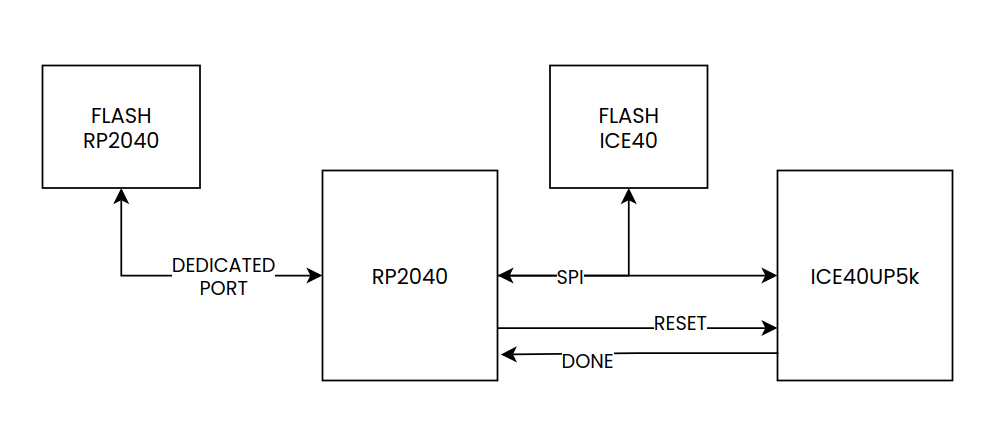
One implementation detail worth noting: in the first version, GPIO8/11/12/13, used for the SPI bus, do not map to the RP2040’s hardware SPI peripheral on those pin positions. The firmware uses a PIO-based SPI implementation (spi_pio.pio) — about 1 MHz for flash programming and approximately 6.25 MHz for TRNG reads. PIO is a good fit here because it is deterministic, timing-accurate, and free from the hardware SPI pin constraints. This will be updated in a future revision to use the hardware SPI peripheral for flash programming, which will speed up updates significantly.
From entropy to conditioned bytes
Raw bits out of the ring oscillators are not ready for cryptographic use. They carry process-level correlations and can show transient bias due to temperature or supply voltage shifts. The RP2040 firmware implements a three-stage pipeline.
Stage 1 — sampling. The RP2040 acts as SPI master and clocks the iCE40 at approximately 6.25 MHz, collecting one raw random bit per SCK clock from the SO line. The iCE40 SPI slave latches a fresh rnd_bit on every falling SCK edge; the RP2040 samples it on the rising edge (SPI Mode 0).
Stage 2 — NIST SP 800-90B health tests. Before any byte enters the output pool, the firmware runs two continuous tests. The Repetition Count Test (RCT) verifies that the same bit value does not repeat beyond a calculated threshold; a long identical run indicates the oscillators have stopped toggling, which would typically mean a latch-up or power supply fault. The Adaptive Proportion Test (APT) examines a 512-bit window and counts the occurrences of the most frequent value; an unusually high count flags a statistical bias condition. If either test fails, the output is paused and the status LEDs signal an error.
Stage 3 — SHA-256 conditioning. Every 16 raw bytes that pass the health checks are fed into SHA-256 to produce 32 conditioned output bytes. A cryptographic hash function is an excellent conditioner: it distributes entropy uniformly across all output bits, so even a biased or partially correlated input produces statistically uniform output as long as there is sufficient total entropy in the input block. The 16→32 byte expansion gives a comfortable margin.
A quick measurement from a 1 Mbit capture on a freshly configured board confirms the output quality:
Shannon entropy : 7.99845 bits/byte   (max 8.00000)
Mean            : 127.45               (ideal 127.5)
Byte freq range : 426–567              (ideal 488)
For production qualification, longer captures should be run through the NIST Statistical Test Suite or dieharder.
The hardware
The board runs entirely from USB bus power. VBUS (5 V) feeds two LDOs: a TLV70233 generates the 3.3 V rail used by the RP2040 I/O, the iCE40 bank I/O and SPI flash chips, while a TLV70212 generates the 1.2 V rail for the iCE40 core and PLL. A polyfuse on VBUS provides overcurrent protection. The RP2040’s internal regulator derives its 1.1 V digital core supply from the 3.3 V rail.
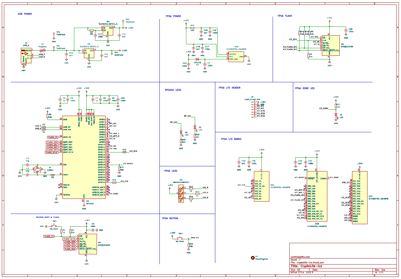
| Ref | Part | Role |
|---|---|---|
| U1 | Lattice iCE40UP5K-SG48ITR | FPGA — 32 ring oscillators + SPI slave |
| U2 | Raspberry Pi RP2040 | MCU — conditioning pipeline + USB |
| U3 | TLV70212 | 1.2 V LDO — iCE40 core + PLL |
| U4 | TLV70233 | 3.3 V LDO — I/O rail |
| U5 | W25Q32JV | 4 MB SPI flash — RP2040 firmware (XIP) |
| U6 | W25Q32JV | 4 MB SPI flash — iCE40 bitstream |
| Y1 | 12 MHz crystal | RP2040 XTAL reference |
| D3 | MHPA1010RGBDT | RGB LED driven by iCE40 (solid green = running) |
The iCE40 RGB LED shows solid green when the bitstream is active. The two RP2040 status LEDs encode the firmware state: solid green on LD2 means idle and ready; fast blinking on both LEDs indicates a random transfer in progress; alternating blink means FPGA flash programming is underway.
The schematic is in the GitHub repository under hardware/.
Getting started
Building the project requires the open-source ICE40 toolchain (yosys, nextpnr-ice40, icepack) for the FPGA bitstream and the Pico SDK for the RP2040 firmware. Python 3 with pyusb covers the host side.
# Clone the repository
git clone https://github.com/controlpaths/cryptoliteICE.git
cd cryptoliteICE

# Provide the Pico SDK (not bundled) and point PICO_SDK_PATH at it
git clone --recurse-submodules https://github.com/raspberrypi/pico-sdk.git
export PICO_SDK_PATH="$PWD/pico-sdk"

# Set up a virtual environment for the host script
python3 -m venv host/.venv
host/.venv/bin/pip install -r host/requirements.txt

# Build the FPGA bitstream (yosys → nextpnr-ice40 → icepack)
bash rtl/build_cryptolite_trng_spi.sh
# → build/cryptolite_trng_spi/cryptolite_trng_spi.bin

# Build the RP2040 firmware (CMake + arm-none-eabi-gcc)
bash mcu/build_criptolite_rp.sh
# → build/criptolite_rp/criptolite_rp.uf2
For the initial flash, put the RP2040 into BOOTSEL mode by holding SW1 while plugging in the USB cable. The board appears as a mass-storage volume:
cp build/criptolite_rp/criptolite_rp.uf2 /media/$USER/RPI-RP2/
sync
Once the RP2040 firmware is running, subsequent FPGA updates require no physical intervention:
# Update the FPGA bitstream over USB
host/criptolite-ice.py update-fpga build/cryptolite_trng_spi/cryptolite_trng_spi.bin
Install the udev rule once to avoid running the host script as root:
sudo cp host/99-cryptolite.rules /etc/udev/rules.d/
sudo udevadm control --reload-rules && sudo udevadm trigger
Requesting random data is then straightforward:
# 32 random bytes as hex, printed to stdout
host/criptolite-ice.py random -n 32

# 1 MB of random data written to a file
host/criptolite-ice.py random -n 1048576 -o rng.bin

# Board status (CDONE, health test results, bytes generated)
host/criptolite-ice.py status
Conclusions
CryptoliteICE is a very tiny device, packed as a USB stick that generates true-random numbers on demand. It demonstrates that a TRNG does not require exotic components or proprietary tooling. The iCE40UP5K contributes physical entropy through ring oscillators, a technique well understood in the literature; the RP2040 provides the intelligence to qualify and condition that entropy before it leaves the device. Neither component is doing anything novel, which is a feature rather than a limitation: a simple, auditable design is preferable in a security context.
This is the first time I have used an ICE40 FPGA, and also the first time I have designed a board for this device, and I am pleasantly surprised that everything works as expected. The FPGA is not too complex to route, especially because of its package, a QFN-48. Although this board uses a 4-layer stackup because of its size, I am fairly sure it could be routed in 2 layers. That said, the 4 layers do help keep the 50 ohm impedance of the clock path.
The schematic, RTL, and firmware are on GitHub under the Apache License 2.0.