Exploring Versal ACAP with the iG-G57D Board
 ig-g57d
I have been using Zynq7000 and Zynq MPSOC devices for years, but I had not had the chance to work with AMD’s latest adaptive platform, Versal ACAP, until now. A few weeks ago, the iWave Global iG-G57D board, based on the Versal AI Edge VE2302, landed into my desk thanks to iWave Global.
I have to say that, when I began to work with this board, I felt that everything changes between Zynq and Versal, but after spending some time with the documentation and the tools, I realized that the core concepts are the same, but there are some differences in the development workflow that can be confusing at first.
A thing that makes me feel more uncomfortable at the very beginning was the concept of the separation of the processing system and the memory controller, and how an AXI DMA will be connected (this will be in a future post). but after reading documentation (Versal ACAP Design Flow, Versal ACAP TRM, Introducing Versal Architecture), I have to say that I think I have a good understanding of the architecture, and then, I read a bit about the AI Engines and everything turns dark again… but I will leave the AI Engines for the future, and I will focus on the PS, PL, CIPS, NoC, and remote debugging (needed if you work from a laptop with 512G of SSD).
Table of contents
- The iG-G57D Board
- The Control & Interface Processing System (CIPS)
- The AXI NoC
- Hardware Design
- Configuring Remote Debugging
- Debugging with Vitis
- Conclusions
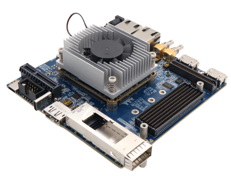
The iG-G57D Board
The iG-G57D is a compact development platform from iWave Global built around the Versal AI Edge VE2302. The VE2302 sits in the mid-range of the AI Edge family and provides a good balance between resource count and power budget.
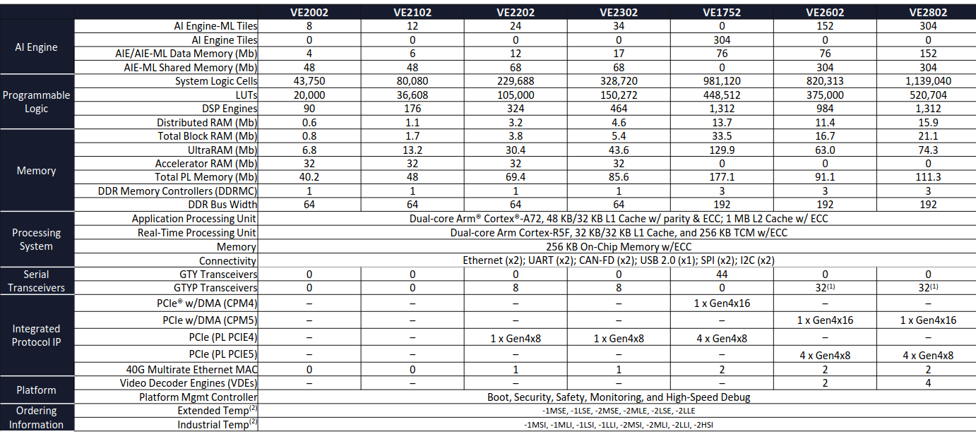
Taking a look at the product selection table, we can see that the VE2302 specifications are:
- AI Engines: 34 AI Engine-ML tiles with 17 MB of AI/ML Data Memory and 68 MB of AIE-ML Shared Memory
- Programmable Logic: 328,720 System Logic Cells, 150,272 LUTs, 464 DSP Engines (DSP58), 85.6 MB total PL Memory
- Processing System: Dual-core Arm Cortex-A72 (APU) and dual-core Arm Cortex-R5F (RPU), 256 KB on-chip memory with ECC
- Peripherals: Ethernet (×2), UART (×2), CAN-FD (×2), USB 2.0 (×1), SPI (×2), I2C (×2)
- Memory: 1× LPDDR4 controller with a 64-bit bus
- High-Speed I/O: 8× GTYP transceivers, 1× PCIe Gen4×8 (PL PCIE4)
The board itself provides 4GB LPDDR4 RAM, Gigabit Ethernet, USB, UART via USB bridge, an FMC+ socket (with the FMC-LPC signals connected for the VE2302), HDMI IN/OUT… and everything we can expect from a development board.
The Control & Interface Processing System (CIPS)
If you have worked with Zynq-7000 or Zynq MPSOC you know the processing_system7 IP. In Versal, that role is played by the Control, Interfaces & Processing System (CIPS) IP.
The difference is not purely cosmetic. The CIPS now encapsulates not only the Processing System — the A72/R5F cores, peripherals, and clocks — but also the Platform Management Controller (PMC), which is responsible for device boot, security, and power management. When you open the customization dialog, it presents two interactive blocks: PS PMC and XRAM.
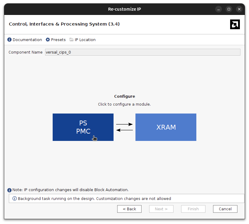
Clicking on the PS PMC block opens a detailed configuration wizard with several tabs that are very similar to the one we find in the Zynq MPSOC, but different enough to spend some time looking for the configurations. Two important tabs are PS PL Interfaces and NoC Interfaces.
PS-PL Interfaces
The PS PL Interfaces tab is where we can configure the AXI connections between the processing system and your programmable logic. The available master and slave interfaces are:
- M_AXI_LPD (Low Power Domain, configurable data width: 32 or 128 bits): the simplest master interface for accessing PL peripherals from the A72/R5F cores. This is the direct equivalent of the Zynq M_AXI_GP ports.
- M_AXI_FPD (Full Power Domain, 128 bits): a higher-bandwidth master interface.
- S_AXI_FPD / S_AXI_FPD2 / S_AXI_LPD: slave interfaces that allow PL masters to access PS resources.
- S_ACP_FPD / S_ACE_FPD: coherent slave interfaces for cache-coherent access from the PL.
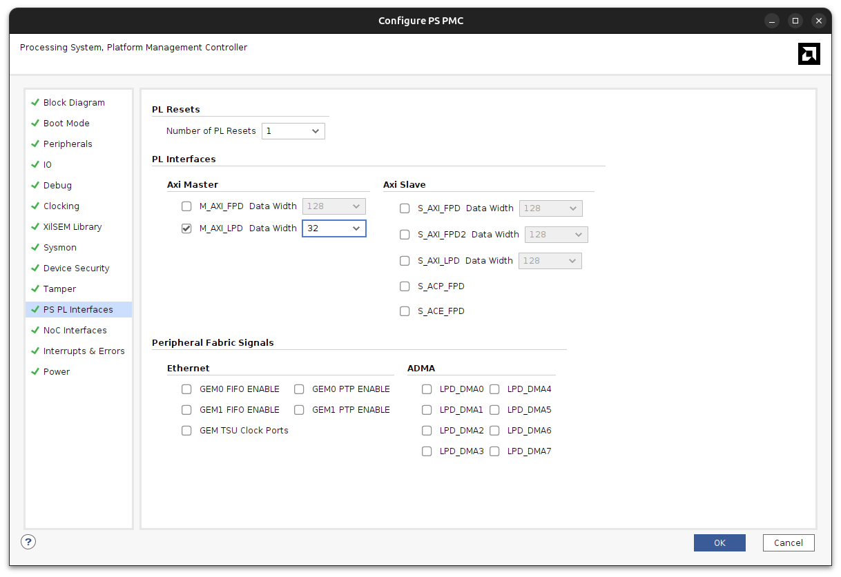
For a simple custom peripheral accessed from a bare-metal application, enabling M_AXI_LPD with 32-bit data width and setting the number of PL Resets to 1 is all that is needed. The CIPS IP will expose the M_AXI_LPD port and the pl0_ref_clk / pl0_resetn signals on the block design canvas.
The AXI NoC
This is the biggest architectural change for anyone coming from Zynq. In Zynq-7000 and Zynq MPSoC, the DDR memory controller is integrated inside the Processing System IP, and PL access to RAM goes through the HP or HPC slave ports of that IP. In Versal, the external memory controller lives inside the AXI NoC, not in the CIPS.
This means that any Versal block design that needs to use external memory — whether from the PS or from the PL — must instantiate the axi_noc IP. There is no way around it.
The AXI NoC provides a high-bandwidth, low-latency switched fabric between multiple AXI master ports and the physical memory controllers. Looking at the block design, you can see several dedicated CIPS-to-NoC interfaces:
- FPD_CCI_NOC_0 through FPD_CCI_NOC_3: Full Power Domain cache-coherent interconnect ports, primarily used by the Cortex-A72 cores for DDR access.
- LPD_AXI_NOC_0: Low Power Domain AXI port, used by the Cortex-R5F and the M_AXI_LPD master when the data must reach DDR rather than a PL peripheral.
- PMC_NOC_AXI_0: PMC access to DDR, used during boot and for secure transactions.
The NoC IP also contains the memory controller (MC) itself. In the VE2302, this connects to LPDDR4 through the CH0_LPDDR4 and CH1_LPDDR4 physical interfaces. The clocks needed by the MC and by downstream IPs (aclk0 through aclk5) are generated and distributed by the NoC as well.
A practical benefit of using a proper board file is that Run Block Automation will configure the entire CIPS + NoC combination automatically: memory type, data width, speed grade, pin assignments, and clock frequencies are all pulled from the board preset. This is a significant time saver compared to setting everything by hand.
Hardware Design
With the concepts clear, here is the step-by-step flow for building a minimal block design that connects a custom AXI4-Lite peripheral to the CIPS via M_AXI_LPD.
Create a new Vivado project as usual (RTL project, do not specify sources), select the Versal AI Edge series, and choose the iG-G57D board preset if it is available in your board repository. If not, which is normal, you will need to add a new Board repository, where the board file is located, and then the board will be available for selection. Once the project is created, add a new block design, then instantiate the CIPS IP. Vivado will offer to run Block Automation — accept it. The automation reads the board preset and adds the AXI NoC with the LPDDR4 memory interface already configured, saving a considerable amount of manual work.
Open the CIPS customization dialog and navigate to PS PMC → PS PL Interfaces. Enable M_AXI_LPD with a 32-bit data width and set the number of PL Resets to 1. Click OK. The M_AXI_LPD port, pl0_ref_clk, and pl0_resetn will now appear on the CIPS block.
For the custom IP, I used the online AXI4 Lite generator to produce a simple register-based adder peripheral. Then, we can instantiate the IP in the block design along with a Processor System Reset and an AXI SmartConnect (1 master, 1 slave) to bridge the M_AXI_LPD bus to the peripheral’s slave AXI port.
In the next image you can see the resulting block diagram.
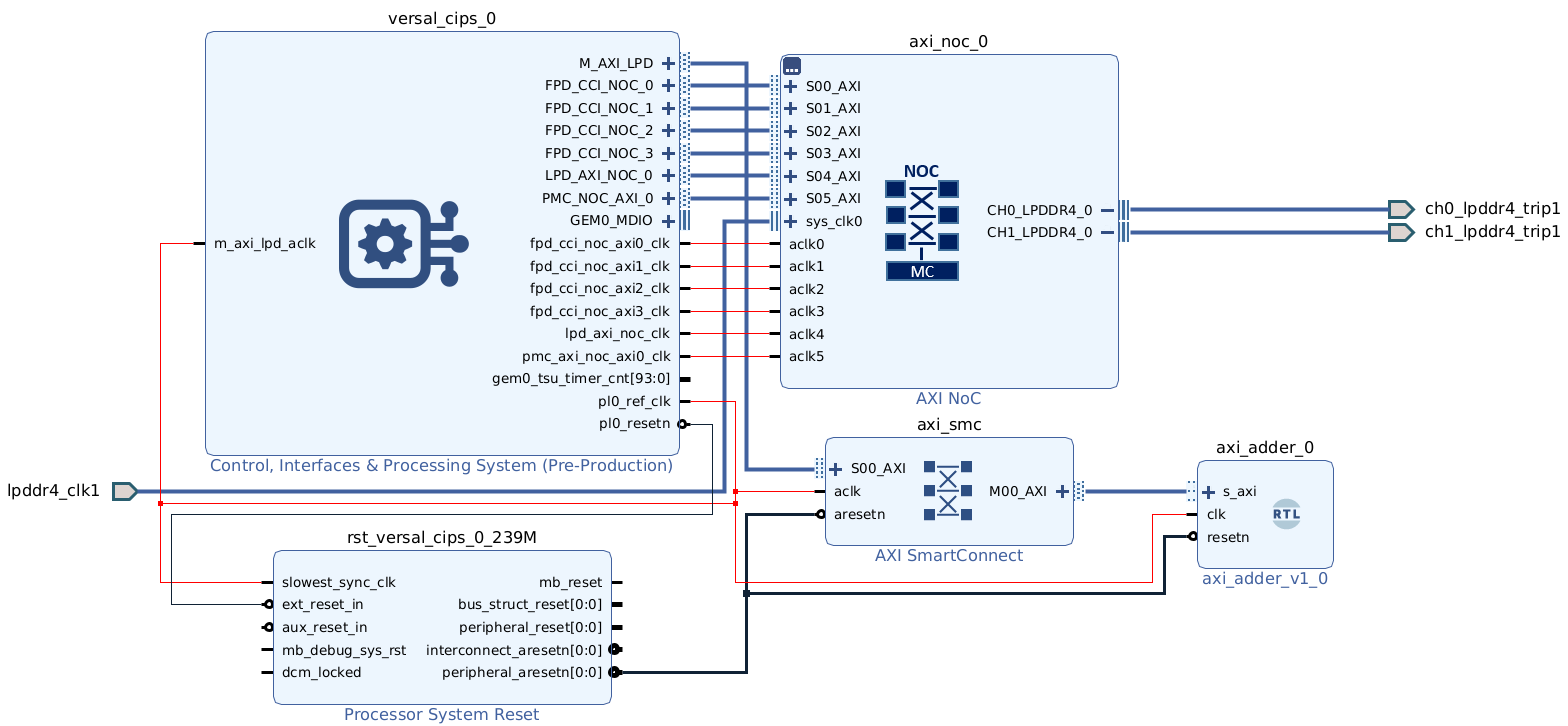
Run Connection Automation to handle any remaining connections, then open the Address Editor. The tool creates two address networks: Network 0 covers the NoC-connected interfaces (used by the A72 cores for DDR), and Network 1 covers the M_AXI_LPD bus.
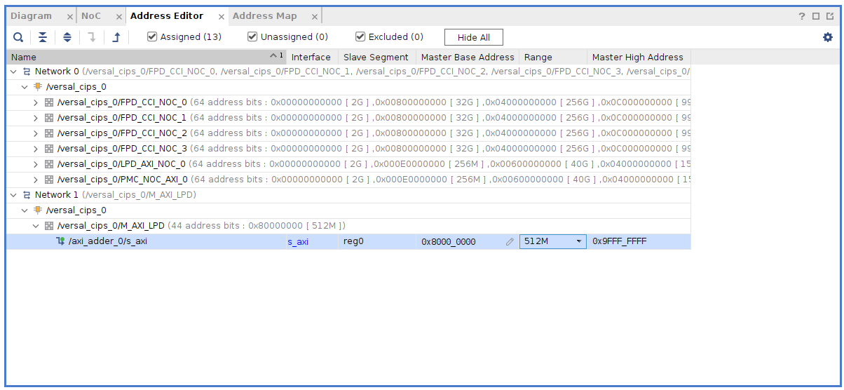
Assign the custom IP slave (/axi_adder_0/s_axi/reg0) a base address of 0x8000_0000 with a 1K range. This puts it at a comfortable distance from the DDR region and within the M_AXI_LPD address space. Validate the design, generate the wrapper, and run synthesis, implementation, and device image generation. Note that Versal does not produce a .bit bitstream — the output is a PDI (Programmable Device Image), which bundles the PL configuration, PS initialization data, and firmware into a single file.
Configuring Remote Debugging
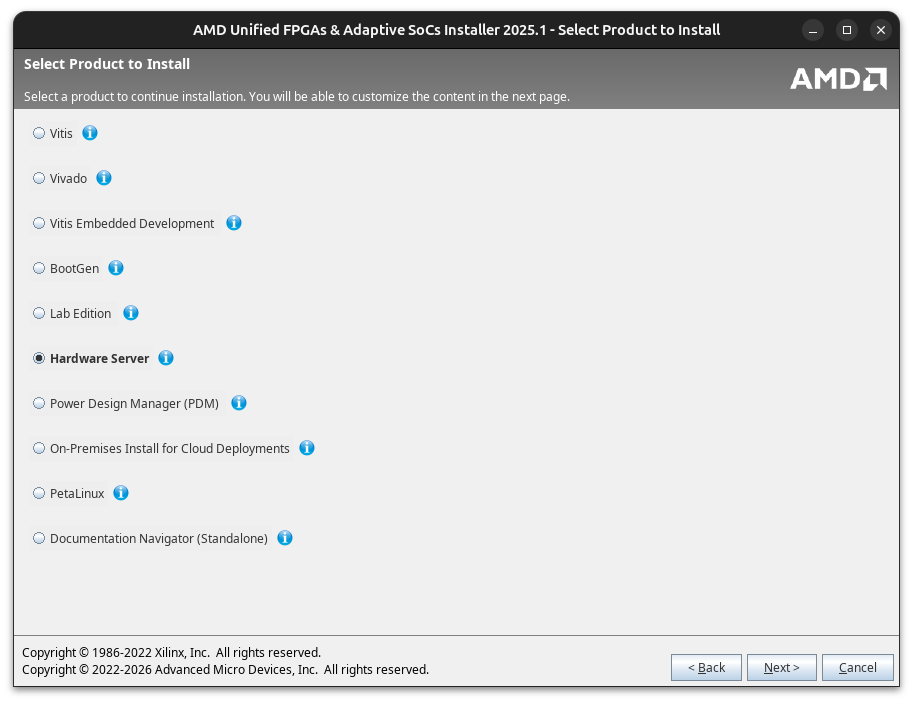
Here is where things get practical. A full Vivado + Vitis installation with Versal device support requires tens of gigabytes of disk space. In my case, I usually work from a laptop, and I have the Vivado installation in a workstation. If I need to debug a design, I would need to connect the board to the workstation, which is not always possible or convenient. Fortunately, we can install a very small part of Vivado in the laptop, called Hardware Server, which allows us to connect the Vivado installation to the board through the network, so we can debug from Vitis without having the full installation on the laptop.
In order to get this tool we just need to launch the Vitis Unified IDE installation, and install the Hardware Server component.
Once it is installed, we can launch the hw_server application on the machine that is physically connected to the board.
../Applications/amd/2025.1/HWSRVR/bin/hw_server
****** Xilinx hw_server v2025.1
**** Build date : May 6 2025 at 15:14:51
** Copyright 1986-2022 Xilinx, Inc. All Rights Reserved.
** Copyright 2022-2025 Advanced Micro Devices, Inc. All Rights Reserved.
INFO: hw_server application started
INFO: Use Ctrl-C to exit hw_server application
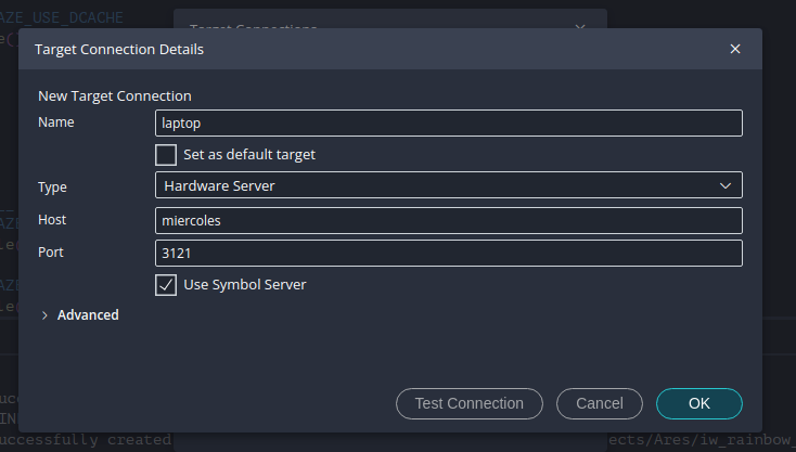
INFO: To connect to this hw_server instance use url: TCP:miercoles:3121
By default it listens on port 3121. The hostname shown (miercoles in my case) is what Vitis will use to connect.
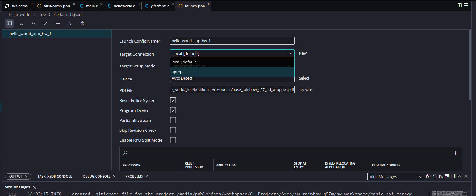
In Vitis, open Target Connections and add a new connection. Set the type to Hardware Server, enter the hostname and port 3121, then click Test Connection.
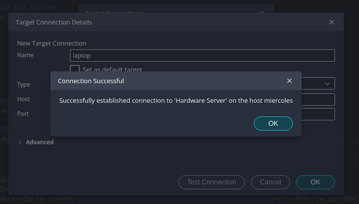
The confirmation dialog confirms the connection is established. From this point on, the remote hardware target (“laptop” in the screenshot, which is the name I gave the connection) appears alongside the local target in any Vitis debug launch configuration.
Debugging with Vitis
With the hardware design exported as an XSA and imported into Vitis as a platform project, create a standard Hello World application. The generated helloworld.c calls init_platform(), prints a message over UART, and calls cleanup_platform(). This is a very simple design but allows me to test the entire chain.
To configure the remote server, open the debug launch configuration. Under Target Connection, select the remote hardware server target instead of the default local connection.
Launch the debug session. Vitis connects to the hw_server on the remote machine, sends the PDI to program the Versal device, loads the ELF, and breaks at main(). Resume execution and open a serial terminal to see the UART output.
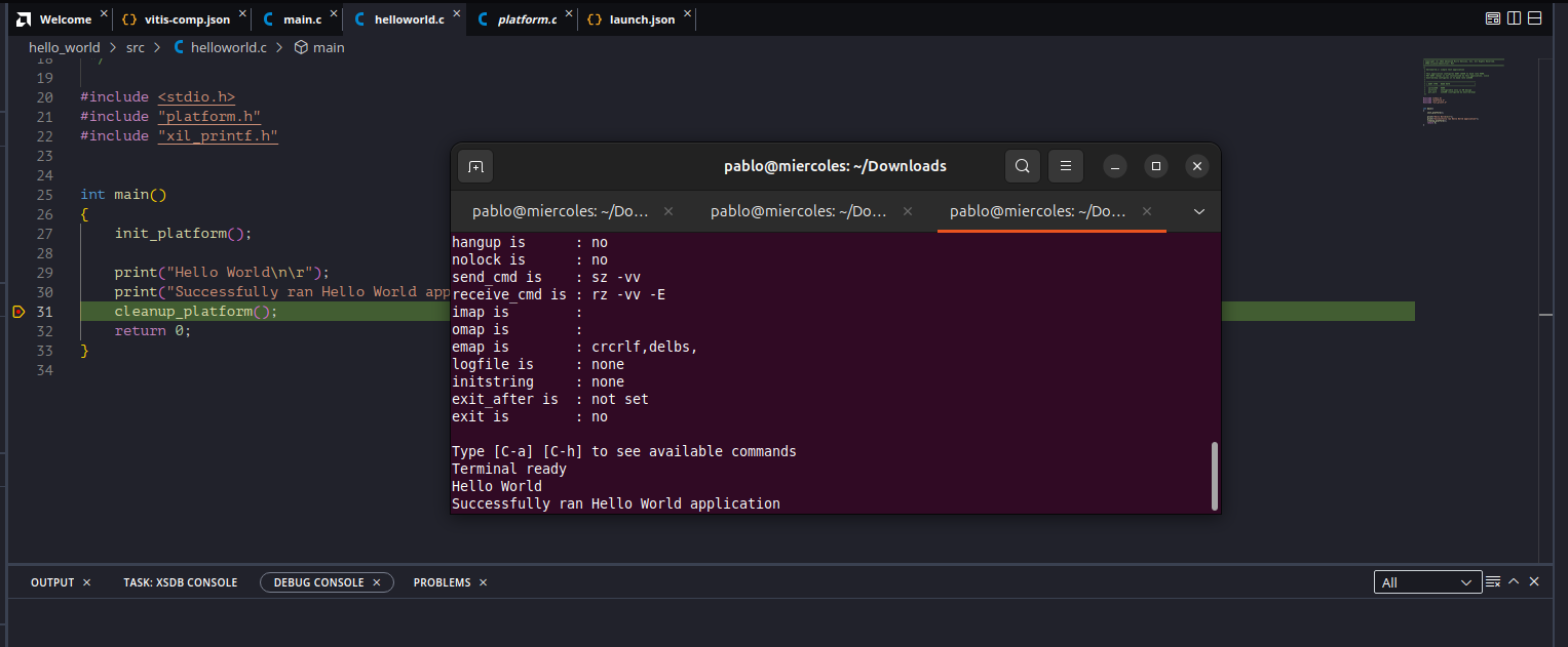
In the terminal we can see that the application ran successfully: “Hello World” followed by “Successfully ran Hello World application”.
Conclusions
As I said in the beginning, the transition from Zynq to Versal is not as drastic as it may seem at first glance (except if you want to use the AIE-ML). The core concepts of a processing system with ARM cores, programmable logic, and AXI interfaces remain, but the introduction of the CIPS and the AXI NoC adds new layers of complexity that require some time to understand.
Regarding the board, I am going to use it for a few projects and also it will be the main character in my talk at the FPGA Developer’s Forum in May.