Getting started with Agilex 3 and floating-point DSP operations

I have been working with Xilinx (now AMD) FPGAs for years, so when the Agilex 3 FPGA and SoC C-Series Development Kit landed on my desk I knew the transition would involve some hard changes. I used Quartus in my University days with a terasic kit based on a Cyclone II and later a Cyclone IV, and I remembered that Quartus, however the current version, 26.1 has nothing similar to that one. Quartus is not Vivado, the terminology differs, and even the project-file philosophy is different.
Regarding the hardware, one feature caught my attention immediately: the Agilex 3 fabric includes Variable Precision DSP blocks that support native IEEE 754 single-precision floating-point multiply-accumulate in hardware, no soft IP required. This is very interesting because Agilex 3 are the cost-effective devices of the Agilex family, however it features this kind of blocks that we can find only in the Versal ACAP devices from AMD.
In this article I will walk through the whole journey: setting up Quartus Prime Pro on Linux, building a trivial LED-blink design to validate the board, and then jumping into a much more interesting project — a three-band Linkwitz-Riley FIR audio crossover that runs entirely in FP32, using the Pmod I2S2 for audio I/O. By the end you will have a clear picture of what the Agilex 3 native floating-point DSP can do for signal-processing workloads.
Table of contents
- The board
- Quartus Prime Pro — a Vivado user’s dictionary
- Setting up Linux for USB Blaster III
- Project 1 — LED blink
- Native floating-point DSP on Agilex 3
- Project 2 — FP32 audio crossover
- Conclusions
The board
The development kit is the Agilex 3 FPGA and SoC C-Series Development Kit , built around the A3CW135BM16AE6S device. It features an Agilex 3 FPGA fabric with a dual-core Arm Cortex-A55 HPS (Hard Processor System) and LPDDR4 memory accessible through HPS EMIF. For this article I only use the FPGA fabric side, but having the HPS available opens the door for Linux-based control in a future post.
The board comes with a 100 MHz reference clock (hvio_pllrefclk on pin AJ27), two user LEDs, a pushbutton reset, and what makes the I2S project possible: a Raspberry Pi HAT GPIO header, that shares some pins with a PMOD compatible connector. That header gives us direct access to 3.3-V LVCMOS I/O pins, which is exactly what the Digilent Pmod I2S2 expects.
Quartus Prime Pro — a Vivado user’s dictionary
If you come from the Xilinx/AMD ecosystem, the first thing you will notice is that Quartus uses a different vocabulary for concepts that are essentially the same. Here is a quick translation table to save you the initial confusion:
| Vivado concept | Quartus equivalent | Notes |
|---|---|---|
.xpr project file |
.qpf project file |
Both store the project metadata |
.xdc constraints |
.sdc + pin TCL / .qsf |
SDC handles timing; pin assignments go in the .qsf or a separate TCL script |
Block Design (.bd) |
Platform Designer (.qsys) |
Graphical IP integration tool |
| IP Catalog | IP Catalog | Same idea, different IP library |
Bitstream (.bit) |
SRAM Object File (.sof) |
Programming file for volatile configuration |
The most important difference for day-to-day work is that Quartus separates timing constraints (SDC) from pin assignments. In Vivado, your .xdc file contains both create_clock and set_property PACKAGE_PIN commands. In Quartus, timing lives in the .sdc file while pin assignments end up in the .qsf settings file or in a dedicated TCL script that is sourced at project-creation time. This separation is actually cleaner once you get used to it.
Setting up Linux for USB Blaster III
The Agilex 3 dev kit enumerates as a USB Blaster III over USB. On a fresh Linux installation, the JTAG daemon (jtagd) will fail to access the device unless you add the proper udev rules. Running lsusb should show something like:
Bus 001 Device 014: ID 09fb:6022 Altera AG3C_SoC_DK
Create the file /etc/udev/rules.d/51-usbblaster.rules with rules for all USB Blaster variants:
# USB Blaster
SUBSYSTEM=="usb", ATTR{idVendor}=="09fb", ATTR{idProduct}=="6001", MODE="0666"
SUBSYSTEM=="usb", ATTR{idVendor}=="09fb", ATTR{idProduct}=="6002", MODE="0666"
SUBSYSTEM=="usb", ATTR{idVendor}=="09fb", ATTR{idProduct}=="6003", MODE="0666"

# USB Blaster II
SUBSYSTEM=="usb", ATTR{idVendor}=="09fb", ATTR{idProduct}=="6010", MODE="0666"
SUBSYSTEM=="usb", ATTR{idVendor}=="09fb", ATTR{idProduct}=="6810", MODE="0666"

# USB Blaster III (Agilex 3 dev kit)
SUBSYSTEM=="usb", ATTR{idVendor}=="09fb", ATTR{idProduct}=="6020", MODE="0666"
SUBSYSTEM=="usb", ATTR{idVendor}=="09fb", ATTR{idProduct}=="6022", MODE="0666"
SUBSYSTEM=="usb", ATTR{idVendor}=="09fb", ATTR{idProduct}=="6024", MODE="0666"
SUBSYSTEM=="usb", ATTR{idVendor}=="09fb", ATTR{idProduct}=="6025", MODE="0666"
SUBSYSTEM=="usb", ATTR{idVendor}=="09fb", ATTR{idProduct}=="6026", MODE="0666"
Then reload and apply the rules:
sudo udevadm control --reload-rules
sudo udevadm trigger
sudo killall jtagd
After this, quartus_pgm and the Quartus GUI programmer should detect the device without root privileges.
Project 1 — LED blink
Before touching floating-point DSP, it makes sense to validate the most basic workflow: create a project, compile, program. The classic LED blinker does the job.
The project uses a TCL script that sets up the device, source files, and constraints in a single reproducible step. Here is the core of scripts/create_project.tcl:
package require ::quartus::project

set PROJECT_NAME  agilex3_base
set REVISION_NAME agilex3_base

if { [project_exists $PROJECT_NAME] } {
  project_open -revision $REVISION_NAME $PROJECT_NAME
} else {
  project_new -revision $REVISION_NAME $PROJECT_NAME
}

set_global_assignment -name FAMILY "Agilex 3"
set_global_assignment -name DEVICE A3CW135BM16AE6S
set_global_assignment -name TOP_LEVEL_ENTITY top
set_global_assignment -name PROJECT_OUTPUT_DIRECTORY output_files

set_global_assignment -name SYSTEMVERILOG_FILE rtl/top.sv
set_global_assignment -name VERILOG_FILE       rtl/led_counter.v

set_global_assignment -name SDC_FILE constraints/timing.sdc
To execute this file from the terminal, we need first to add the Quartus executables to the path. In a similar way that we execute the script settings64.sh to have vivado added to the path, we have a similar script in the Quartus installation folder.
source ~/Applications/altera_pro/26.1/qinit.sh
After executing this script, we have access to tools like quartus_sh for a terminal based application, quartus for the gui application, or quartus_pgm for programming.
Running quartus_sh -t scripts/create_project.tcl creates the .qpf and .qsf files. From there, open the project in Quartus Prime Pro 26.1 and click on Start Compilation.
The top-level module instantiates a led_counter module that divides the 100 MHz clock down to a 100 ms tick and drives a 2-bit counter:
module top (
  input hvio_pllrefclk,
  input io96_3a_pb1_fpga_rst_n,
  output io96_3a_led0,
  output io96_3a_led1
);

  wire [1:0] led_count;

  led_counter u_led_counter (
    .aclk(hvio_pllrefclk),
    .resetn(io96_3a_pb1_fpga_rst_n),
    .led(led_count)
  );

  assign io96_3a_led0 = led_count[0];
  assign io96_3a_led1 = led_count[1];

endmodule
The pin assignments for this project are straightforward:
| Signal | Pin | IO Standard | Description |
|---|---|---|---|
hvio_pllrefclk |
AJ27 | 3.3-V LVCMOS | 100 MHz reference clock |
io96_3a_pb1_fpga_rst_n |
M1 | 1.1 V | Active-low reset (pushbutton PB1) |
io96_3a_led0 |
K1 | 1.1 V | LED0 — counter bit 0 |
io96_3a_led1 |
L2 | 1.1 V | LED1 — counter bit 1 |
After compilation, the bitstream lands in output_files/. To program from the command line:
quartus_pgm -m jtag -o "output_files/agilex3_base.sof"
If the LEDs start cycling through the four binary states, the toolchain is working end to end and it is time to move on to something more interesting.
Native floating-point DSP on Agilex 3
Most FPGAs handle DSP workloads in fixed-point: you carefully choose your Q format, manage bit-widths at every stage, and pray the rounding errors stay acceptable. The Agilex 3 family offers an alternative. The Variable Precision DSP blocks in the fabric include a native IEEE 754 single-precision (FP32) mode that performs multiply-accumulate operations in hardware.
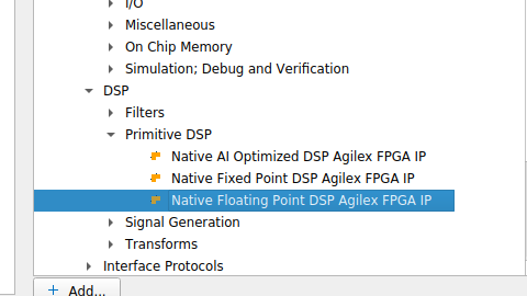
The specific IP used in this project is the Native Floating Point DSP Agilex FPGA IP, which maps to the tennm_fp_mac primitive. It is important to select the correct IP from the catalog — it lives under DSP → Primitive DSP, not under the soft Floating Point Functions:
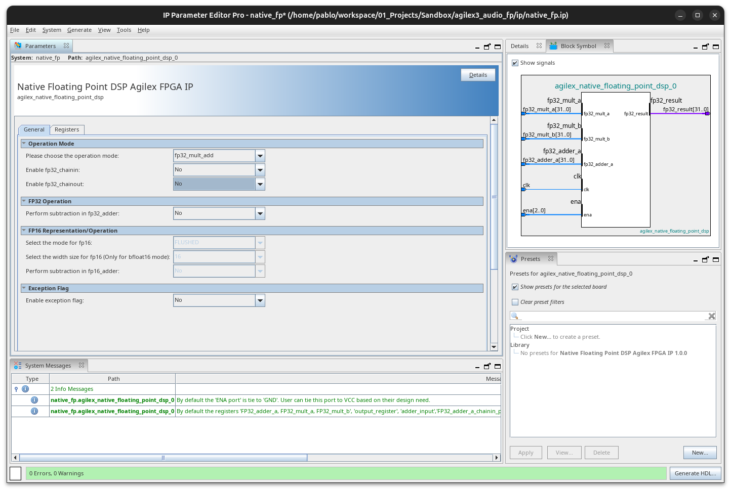
The IP Parameter Editor shows the configuration used in this project: fp32_mult_add operation mode, with chain-in and chain-out disabled:
This is not the soft Floating Point Functions FPGA IP that synthesises FP operations from LUTs; it is a hard silicon path inside the DSP block. The difference matters: the native IP runs at full clock speed with deterministic latency and consumes no fabric logic for the arithmetic itself.
The internal architecture of the DSP block in multiply-add mode is shown in the following diagram from the Altera documentation. You can see the input register bank, the FP32 multiplier with its pipeline stages, the adder, and the output register — these are the five pipeline stages that give the 5-cycle latency:
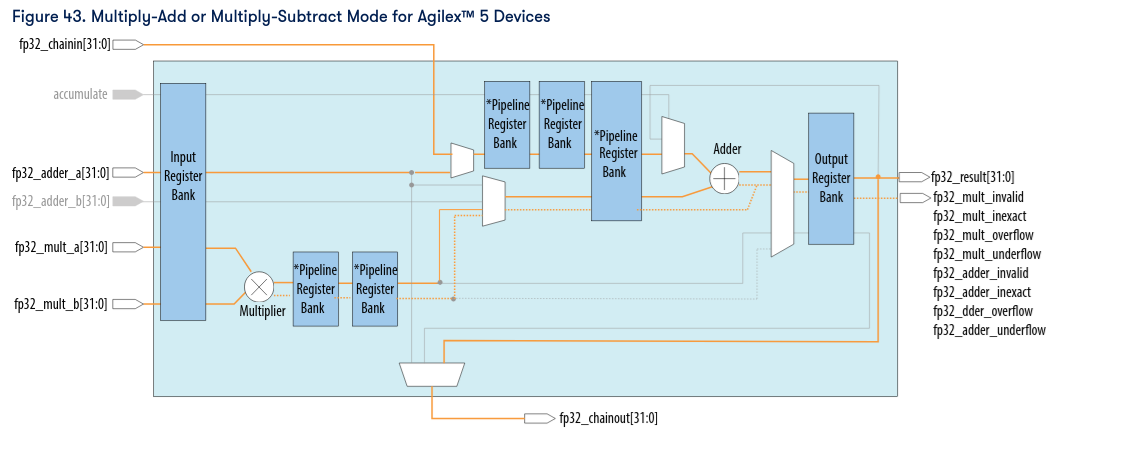
In fp32_mult_add mode, the IP computes:
Where \(a\), \(b\), and \(c\) are all IEEE 754 FP32 values. With all pipeline registers enabled (ena = 3'b111), the latency is 5 clock cycles: input register, multiplier pipeline stage 1, multiplier pipeline stage 2, adder input register, and output register. This predictable latency makes it straightforward to build time-shared architectures around it.
Project 2 — FP32 audio crossover
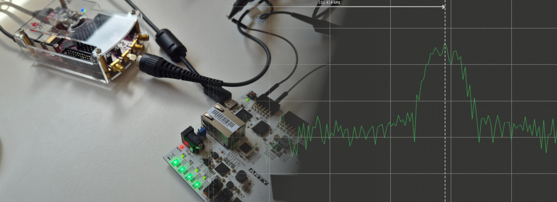
With the toolchain validated, the second project puts the native FP DSP blocks to real use. The goal is to build a three-band Linkwitz-Riley order-3 (LR3) FIR audio crossover that splits a stereo audio stream into bass, mid, and high frequency bands, all processed in FP32. Audio I/O is handled by a Digilent Pmod I2S2 module connected to the PMOD compatible connector on the dev board.
Linkwitz-Riley crossover basics
A Linkwitz-Riley crossover is a standard technique in professional audio to split a signal into frequency bands without introducing amplitude dips or peaks at the crossover frequency. An LR crossover of order \(N\) is formed by cascading two Butterworth filters of order \(N/2\) (for even orders), or by using an equivalent design that produces the characteristic flat magnitude sum.
This design approximates LR3 behaviour using linear-phase FIR filters with 63 taps and a Kaiser window (\(\beta = 8.6\)). Three separate filter bands cover the audio spectrum:
| Band | Pass region | Taps | FP32 ROM entries |
|---|---|---|---|
| BASS | 0 – 250 Hz | 63 | BASS[0..62] |
| MID | 250 Hz – 3 kHz | 63 | MID[0..62] |
| HIGH | 3 kHz – 24 kHz | 63 | HIGH[0..62] |
The advantage of FIR filters here is that they preserve linear phase, which means all three bands stay time-aligned at the output. With the LR magnitude response, the three bands sum flat across the spectrum — exactly what you want in a crossover.
System architecture
The following diagram shows the complete signal path, highlighting the boundary between the 24-bit fixed-point I/O stages and the single-precision floating-point processing core:
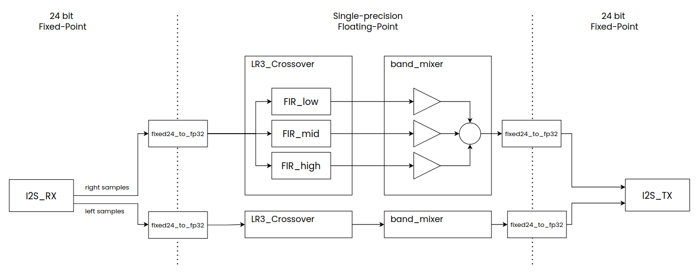
Audio arrives from the CS5343 ADC on the Pmod I2S2 as a 24-bit I2S stream. The i2s_rx module deserialises it into left and right 24-bit samples. These are converted to FP32, fed through independent left/right crossover instances, mixed with per-band gain control, converted back to 24-bit fixed-point, and serialised out to the CS4344 DAC.
The module hierarchy reflects this signal flow:
top.sv
├── mclk_gen.v            — generates MCLK, BCLK, LRCK from 100 MHz
├── i2s_rx.v              — receives 24-bit L+R samples from CS5343
├── fixed24_to_fp32.v     — converts signed 24-bit to IEEE 754 FP32
├── lr3_crossover.v       — 3-band FIR crossover (×2: left + right)
│   ├── fir_fp32.v        — 63-tap time-shared FP32 FIR (×3 per channel)
│   │   └── native_fp     — Agilex Native FP DSP IP (×3 per channel)
│   └── coeff_rom.v       — band-selected coefficient ROM (×3 per channel)
├── band_mixer.v          — per-band FP32 gain + sum (×2: left + right)
├── fp32_to_fixed24.v     — converts FP32 back to signed 24-bit
└── i2s_tx.v              — serialises 24-bit L+R to CS4344
FP32 FIR filter implementation
Each FIR filter instance (fir_fp32) is a direct-form structure with a 63-element delay line. Instead of instantiating 63 multiplier-accumulators, the design time-shares a single native_fp instance across all taps. The accumulator feedback loop works as follows: the FP32 result of the previous tap feeds back as the fp32_adder_a input of the next multiply-accumulate, stored in a 32-bit register. There is no DSP chain-in/chain-out between blocks; a single IP instance processes one tap every 6 clock cycles.
The core MAC instantiation in fir_fp32.v:
native_fp u_mac (
  .fp32_mult_a  (delay_line[tap_idx]),
  .fp32_mult_b  (coeff_data),
  .fp32_adder_a (acc),
  .clk          (aclk),
  .ena          (3'b111),
  .fp32_result  (mac_result)
);
The state machine walks through taps 0 to 62, waiting 5 cycles for the pipeline to produce each result, then capturing it into acc and advancing to the next tap. The total processing time per sample is 63 taps × 6 cycles = 378 clock cycles. At 100 MHz with a sample rate of ~48.8 kHz, there are approximately 2,048 clock cycles available per sample, so the filter uses about 18% of the budget. Three parallel filters (bass, mid, high) run simultaneously, each on its own native_fp instance, so the per-channel budget stays at 378 cycles.
if (phase == LATENCY[2:0]) begin
  acc <= mac_result;
  phase <= 3'd0;
  if (tap_idx == TAPS - 1) begin
    computing <= 1'b0;
    sample_out <= mac_result;
    out_valid <= 1'b1;
  end else begin
    tap_idx <= tap_idx + 6'd1;
  end
end else begin
  phase <= phase + 3'd1;
end
The FIR coefficients are generated by a Python script, which uses SciPy’s firwin function with a Kaiser window. The script outputs Verilog localparam hex literals for BASS, MID, and HIGH bands that are pasted directly into coeff_rom.v. Regenerating coefficients is a one-liner:
Band mixer and gain control
After the crossover, a band_mixer module applies an individual FP32 gain to each band and sums them:
I2S audio interface and clocking
The Pmod I2S2 contains a Cirrus Logic CS5343 ADC and CS4344 DAC, both of which expect I2S timing signals from the FPGA. The mclk_gen module divides the 100 MHz system clock to produce the required audio clocks:
| Clock | Division | Frequency |
|---|---|---|
| MCLK | ÷4 | 12.5 MHz |
| BCLK | ÷16 | 3.125 MHz |
| LRCK | ÷1024 | ~48.8 kHz |
These clocks are output through the PMOD compatible connector. The Pmod I2S2 module is wired to the header as follows:
| HAT GPIO | Signal | Pmod I2S2 pin |
|---|---|---|
| GPIO20 | MCLK | J1-1 |
| GPIO21 | LRCK | J1-2 |
| GPIO22 | DAC_SDATA | J1-3 |
| GPIO24 | BCLK | J1-4 |
| GPIO25 | ADC_SDATA | J1-7 |
| GND | GND | J1-5 / J1-11 |
| 3.3V | VCC | J1-6 / J1-12 |
Timing analysis — clock launch delay
When I first reviewed the timing report, I noticed a clock launch delay of more than 4.5 ns on some paths. That is a large number, and at first I suspected the global clock buffers were not being used — a large clock network delay often means the signal is routed through local interconnect instead of the dedicated clock tree.
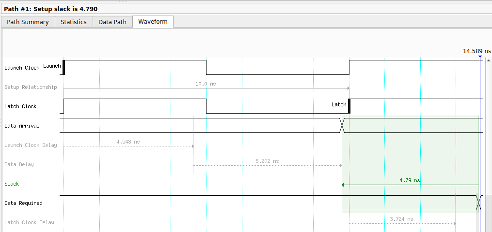
I added constraints in the SDC file to force the use of global clock paths, but the delay did not decrease. Looking at the data path detail, we can see how those 4.5 ns are distributed — and notably, the input buffer for hvio_pllrefclk has an excessive fanout of more than 4,000 nodes:
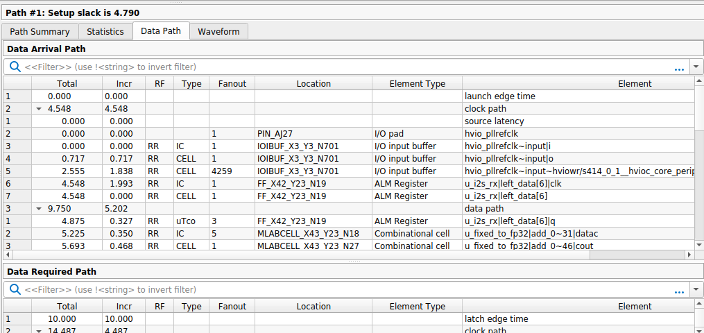
After further investigation I realised the large launch delay was dominated by the input pin delay, because the clock enters through an I/O pad rather than a PLL input. If you look at the internal register-to-register paths, the clock delay is around 0.05 ns, which confirms the global clock tree is working correctly. The take-away: a few nanoseconds of clock insertion delay at the I/O boundary is normal for Agilex 3 when using a pad-sourced clock, and it does not indicate a routing issue.
Verifyig the use of DSP blocks, not LUTs
The whole point of using the native_fp IP is to push the floating-point arithmetic into dedicated DSP silicon rather than consuming fabric LUTs. After compilation, the Quartus resource usage report confirms that the FP32 MAC operations are mapped to Variable Precision DSP blocks and not to ALMs. The design instantiates 12 native_fp instances (3 FIR filters × 2 stereo channels + 3 Gains × 2 stereo channels ), each occupying one DSP block. The coefficient ROMs, delay lines, and control logic use a modest amount of ALMs and M20K memory, but the heavy computation runs entirely in the DSP hard blocks.
This is a significant advantage over soft floating-point IP. A soft FP32 multiplier typically consumes hundreds of ALMs and runs at a lower clock frequency. The native DSP approach uses zero ALMs for the arithmetic, runs at the full fabric clock, and has deterministic latency.
Conclusions
I always say that, if you know how to use one FPGA, you know how to use every FPGA. Vivado, Quartus, Libero SoC, Diamond — all of them are different, but in the end, all of them have VHDL/Verilog source code, a constraints file for clock constraints, pin constraints, a way to draw the circuit, a set of IPs that can be added to the drawing or instantiated into the source code. Each one has its particularities, yes, but it is not too hard to switch between one and another.
As I mentioned at the beginning of the article, this is the first time I have used an Agilex FPGA, and I have to say that I like them a lot. They are pretty new FPGAs — the Agilex family was born in 2023 and became available in 2024 — and this youth means they include some interesting features from the start.
The floating-point DSP is one of them, but executing this kind of operations is not the only thing these blocks can do. They are optimised to work in combination, so they can execute matrix multiplications in a few cycles — an operation that is very important in the AI field.
The board I have features an SoC that includes a Hard Processor System (HPS), a dual-core Arm Cortex-A55, so in the next articles we will take a look at it.