Internal USB header JTAG cable with an FT232H

I am a great fan of buying cheap FPGA accelerator cards and repurposing them for experiments and custom workloads. Now, I have a computer where I test this boards and use it as a development platform for various projects. However, I always need to have a JTAG cable that goes from a USB connector outside the case to the internal card, which is not ideal.
A few days ago, using the AS20MC04 board, I realized that I have one USB 2.0 header free on the motherboard, and I thought: can I build a small adapter that plugs into that header and provides JTAG to the internal card? The answer is absolutely!
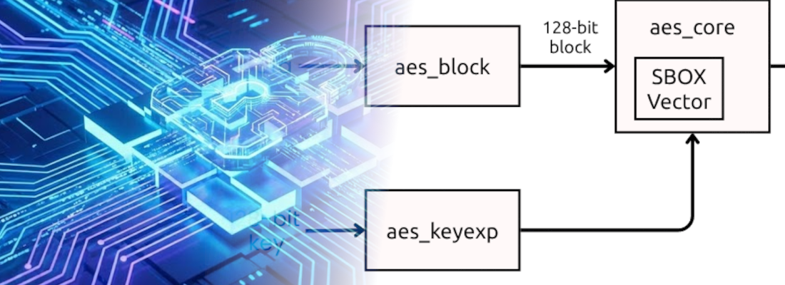
In order to develop our own JTAG cable, we have several options. The first one is to buy a commercial USB-to-JTAG adapter and hack it (for example, cutting the USB cable and re-wiring it to an internal header). The second option is to build our own from scratch using a microcontroller with USB support, like the RP2040. The third option is to use an FTDI chip with MPSSE support, which is what I chose for this project.
In this article, we build a small adapter board around an FT232H that plugs into the motherboard’s internal USB 2.0 header (the 2×5, 10-pin connector used for front-panel USB). From there, it generates a JTAG interface for the accelerator card fully inside the computer, avoiding a USB cable going outside the case.
Table of contents
- Motivation and goals
- Hardware design
- Schematic and layout notes
- Software setup (Vivado) and FTDI EEPROM programming
- Conclusions
Motivation and goals
Development boards usually expose a JTAG connector at the edge of the PCB, so you can connect a cable and you are done. But many accelerator boards and NIC-style FPGA cards don’t expose JTAG at all (only test pads), expose it on a tiny unpopulated header, or place it in an area that becomes inaccessible once the card is installed (facing the chassis, covered by a GPU, or blocked by airflow hardware).
If the board is internal and you rely on an external USB JTAG cable, you typically end up either keeping the side panel open and routing a cable outside (annoying and fragile), removing the card every time you need to program it (slow and risky), or investing early effort in a non-JTAG configuration path (often the right end-state, but not ideal when you are still doing bring-up).
This adapter is meant to keep the fast iteration loop during bring-up, while still allowing you to move to a more production-ready flow later.
Concretely, the goal is a board that stays fully inside the PC: USB power and data come from the motherboard’s internal header, and the JTAG cable runs internally to the accelerator card. I also want it to be small and simple (no MCU firmware), electrically robust (stable TCK, correct pulls, solid ground reference), and voltage-aware by using the target’s VREF/VTREF so the adapter matches 1.8 V / 2.5 V / 3.3 V JTAG banks. Finally, it should fail safely: a wiring mistake should not take down the motherboard USB port or damage the FPGA card.
Hardware design
FT232H and MPSSE basics
The FT232H is a USB 2.0 High-Speed (480 Mbps) USB-to-serial/FIFO chip. The feature we care about is MPSSE (Multi-Protocol Synchronous Serial Engine), which can drive JTAG/SPI/I²C-like protocols with decent performance.
Conceptually, the PC speaks USB to the FT232H, the FT232H toggles the JTAG pins in a controlled way (TCK, TMS, TDI) while sampling TDO, and Vivado’s hw_server uses that interface to implement the TAP controller and drive the programming/debug flow.
You can do many “bring-up sanity checks” with just this: detect the chain, read IDCODEs, check IR lengths, and verify that the physical wiring is correct before you even attempt programming.
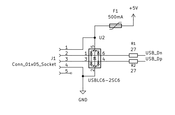
USB header connection (10-pin)
Most ATX motherboards provide one or more internal USB 2.0 headers for front-panel USB ports. The classic connector is a 2×5 header with one key pin missing.
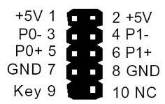
A typical header exposes two USB 2.0 ports on the same 2×5 connector (each port provides VBUS, D-, D+, and GND), plus a “key” position (missing pin) or an NC pin. In this design I only use one of those ports, and the motherboard connection is a small right-angle 1×5 socket (J1) that makes the mechanical assembly neat inside the chassis.
JTAG electrical interface (VREF, level shifting, pulls)
JTAG is “simple” logically, but it is easy to make it flaky electrically if you ignore the details.
The key decision is I/O voltage. Many FPGA boards expose a JTAG VREF pin (sometimes called VTREF) that tells the cable what logic level the target expects. In this board I did not try to run the FT232H I/O bank directly from VREF; instead, I kept the FT232H side at +3V3 and used a small level translator (TXB0104D) so the JTAG pins presented to the target follow VREF. This prevents the classic mistake of driving 3.3 V logic into a 1.8 V JTAG bank.
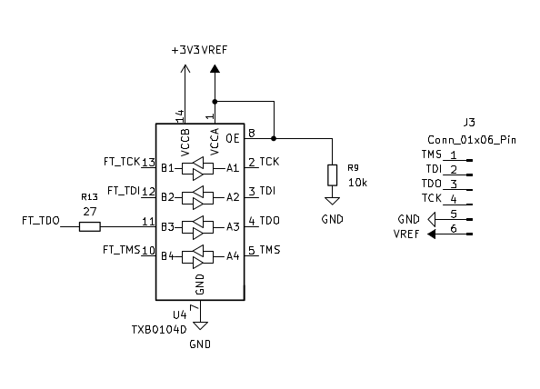
The important rule is that VREF is a reference, not a power rail. The adapter should not attempt to “power the target” through VREF; it should only sense it and use it to set the output levels, either by feeding VCCIO on a compatible cable - only valid for 3.3 targets- , or by powering the A-side of a translator as I do here.
From a signal-integrity perspective, a clean ground reference and conservative edges matter more than high speed. In this revision I added 27 Ω series resistors on the JTAG interface (R10–R13), which helps damp ringing and makes the adapter more forgiving with short internal harnesses. If you still see intermittent detection, keep the internal cable short and reduce the JTAG clock.
If your accelerator board does not expose VREF, you can still do this project, but you must decide what voltage to use and confirm it matches the board’s JTAG bank.
Connecting to the accelerator card
The “other half” of this project is getting JTAG onto the accelerator card in a way that is still usable when the card is installed.
In practice, I often see one of these situations: the card has an unpopulated JTAG header footprint (best case, you can solder a low-profile header), the card exposes test pads (you can solder thin wires, or build a pogo-pin jig), or the card routes JTAG through some mezzanine connector that becomes unreachable once installed. In all cases, what matters is that you can reliably reach TCK, TMS, TDI, TDO, and GND (and ideally VREF).
If you are routing a short internal cable, keep it as short as possible and include at least one ground next to the signals (for example, a ribbon where every other wire is GND, or a small twisted pair for TCK+GND).
Schematic and layout notes
At a block level, the USB input comes from the motherboard header through the polyfuse (F1) and the ESD protection (U2), and then into the FT232H (U1). USB D+/D- are routed with small series resistors (R1/R2) to tame edges and reduce ringing, which is especially useful when the “cable” is a short internal harness rather than a well-controlled external USB cable.
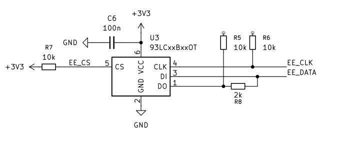
The FT232H needs a clock source, so the board includes a crystal (Y1) with its load capacitors (C7/C8). On the configuration side, the schematic also includes an external EEPROM (U3, 93LCxx series) connected to the FTDI EEPROM pins (EE_CS, EE_CLK, EE_DATA). This is relevant for the Vivado flow, because it is where the USB descriptors live after using program_ftdi.
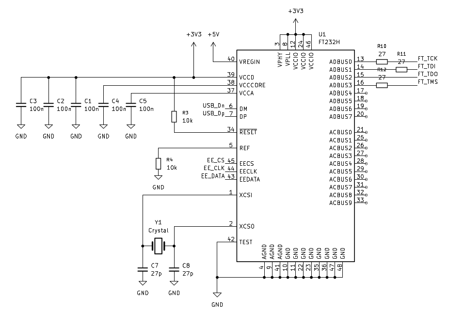
As I mentioned before, for voltage compatibility, I kept the FT232H side at +3V3 and translated the JTAG signals with a TXB0104D level translator (U4). The nets are explicit in the schematic: the FTDI-side signals are FT_TCK, FT_TMS, FT_TDI, FT_TDO, and the target-side signals are TCK, TMS, TDI, TDO going to the JTAG header (J3), together with VREF and GND. With this approach, VREF is used as the “target logic” reference for the translator, instead of trying to run the FT232H I/O bank directly from the target voltage.
Suggested JTAG pinout
If you control both ends (adapter and a small cable to the accelerator), a compact 1×6 header is convenient. At minimum, carry TCK, TMS, TDI, TDO, GND, and VREF, and add another ground if you can. If you include TRST and SRST, keep them pulled to the inactive state by default.
On the layout side, route D+/D- as a short, tight differential pair and place ESD protection close to the connector. Keep the JTAG traces short and away from switching regulators, put the series resistors close to the source, and give yourself test points for TCK and TDO so you can quickly debug a dead chain. Mechanically, internal headers often have limited clearance with GPUs and airflow shrouds, so a right-angle 2×5 shrouded header tends to make the assembly more robust.
One small practical note about TXB010x-style translators: they don’t like strong external pull-ups or long, high-capacitance cables. Keeping the internal JTAG cable short, using weak bias resistors (like the 10 kΩ network in the schematic), and reducing the JTAG clock if you see intermittent detection makes the setup much more reliable.
Software setup (Vivado) and FTDI EEPROM programming
For this project, the “nice” end goal is to have the adapter show up as a cable that Vivado can talk to through hw_server, so you can use the normal Hardware Manager flow to program and debug Xilinx FPGAs.
In practice, that comes down to two questions: does your FTDI chip model match what Vivado supports as a JTAG cable, and does the device present the expected USB identifiers and descriptors. The second part is what FTDI EEPROM programming is for.
AMD documents official Vivado Hardware Manager support for FTDI devices, as long as the FTDI EEPROM is programmed with the program_ftdi utility that ships with Vivado. The supported devices include FT232H, FT2232H, and FT4232H, and once programmed they are recognized as valid programming cables in Vivado. For reference, you can take a look to the UG908 section “Programming FTDI Devices for Vivado Hardware Manager Support”.
Programming the FTDI EEPROM with program_ftdi
Vivado includes a utility called program_ftdi that can write the FTDI EEPROM so the device enumerates with the IDs and descriptors Vivado expects. The important part is not “branding”; it’s making sure the VID/PID and interface descriptors match what hw_server recognizes.
In order to program the EEPROM, connect the FT232H-based adapter to your PC (through the internal USB header), then, from Vivado TCL console execute:
program_ftdi
For example, to program an FT232H as a JTAG cable, you would run:
program_ftdi -write -ftdi FT232H -serial 0ABC01 -vendor "vendor name" -board "my board" -desc "my product description"
Verifying in Vivado Hardware Manager
Once the adapter enumerates as expected, start Vivado and open the Hardware Manager. The sanity check is simply that hw_server can see the cable and that the JTAG chain scan returns valid IDCODEs. At that point you can proceed with the usual bitstream programming flow.
If the scan fails, the most common culprits are still electrical: a wrong VREF/VCCIO voltage (so TDO never toggles, or inputs read undefined), TMS/TCK swapped (the chain looks completely dead), missing shared ground between adapter and accelerator, or simply running TCK too fast for a messy internal cable. Reduce the JTAG clock in Vivado/hw_server if you see intermittent detection.
Once you can reliably read the IDCODE(s), you have a solid base to integrate programming into your preferred flow.
Conclusions
I am quite sure some of you are thinking: why not build a bootloader flow, or use a PCIe-to-JTAG IP, or just make the board self-configuring. I agree that those are good long-term options, and I often end up implementing them. But when you are doing bring-up (or when something goes wrong and the board is “stuck”), nothing beats a direct and predictable JTAG interface that you can use to scan the chain, read IDCODEs, and reprogram the device.
The next step is to send the design to fabrication and validate it on real hardware, installed in a PC with an internal PCIe FPGA card. Once I have verified that everything works as expected (including Vivado Hardware Manager detection and reliable programming), I will release the complete design files.