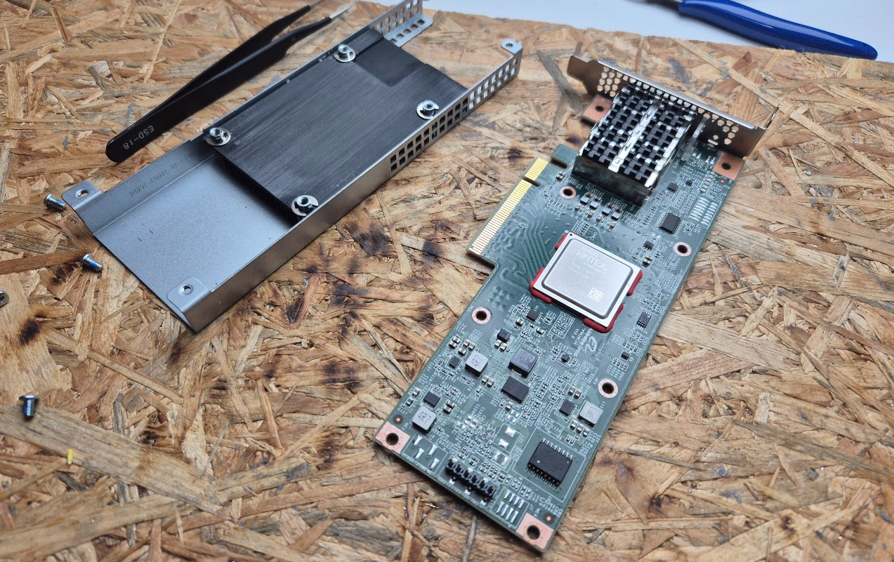
AS02MC04 (Alibaba Cloud) Kintex UltraScale+ NIC

I am not sure if it was Santa Claus or the Three Wise Men (SSMM Los Reyes Magos) who brought it to me, but I finally have one of these interesting little FPGA NIC cards to play with: the AS02MC04 from Alibaba Cloud. This board is built around an AMD/Xilinx Kintex UltraScale+ (XCKU3P). It is a very interesting platform if you want to experiment with high-speed serial links without starting from a custom PCB, and at a very affordable price point (around 200 USD).
In this article we are going to see the essentials to get started with the board: available clocks, the PCIe interface, and the SFP+ transceivers. Then, we are going to focus on the strongest point of this board, the GTY transceivers, and configure the transceivers connected to the SFP+ ports. To do that we are going to use the Ultrascale FPGAs Transceivers Wizard.
Table of contents
- Resources: board files and references
- Board overview
- Clocks
- GT loopback over SFP1 ↔ SFP2
- Data generation and checking
- Conclusions
Resources: board files and references
Let’s make it clear that this is not a development board. This board is meant to be used as a PCIe NIC card in servers, so it does not have the same level of documentation and example designs as a Xilinx development board (like the KCU105 or KCU116). However, there are some useful resources to get you started.
Since it is a NIC card, there are no GPIOs or buttons exposed, so bring-up is mostly about getting the PCIe and GT links working. Fortunately, it has some LEDs that we can use to get feedback from the FPGA.
The most useful starting point I found is this GitHub repository, which includes a Vivado board definition for the AS02MC04, and from the board files we can extract the pinout and clocking information. The README.md also links to a more detailed reverse-engineering write-up by the author.
Board overview
As I said before, this board has no official documentation, so there are no schematics, hardware guides, or reference designs available from AMD or Alibaba Cloud. However, the board definition files in the repository linked above provide a good overview of the main components and pinout.
From the Vivado board definition (as02mc04/1.0/board.xml and as02mc04/1.0/preset.xml), the highlights are:
- FPGA:
xcku3p-ffvb676-2-e(Kintex UltraScale+). - 2× SFP cages exposed as 1-lane GT interfaces (
sfp_1,sfp_2). - PCIe edge connector described up to x8 (board file provides x1/x2/x4/x8 interface modes).
- Reference clocks for both the FPGA fabric and the GTs (details in the next section).
The presets also include the GT placement for the two SFP ports:
- SFP1 is preset to GTY lane
X0Y15(QuadX0Y3) - SFP2 is preset to GTY lane
X0Y14(QuadX0Y3)
This will be important later.
Regarding the PCIe interface, the board file provides pin mappings for the PCIe lanes and reference clock, so you can instantiate a PCIe IP core (for example, the PCIe Gen3 x8 Endpoint core) and connect it to the appropriate pins.
Also, the board has some user LEDs that can be used for feedback during bring-up.
Clocks
Since the board is designed as a NIC card, it includes several reference clocks for both the FPGA fabric and the GT transceivers. According to the board file, the key clocks available are:
- diff_100mhz_clk: 100 MHz differential system clock for the FPGA fabric (connected to
HCLK_CLKpin). - sfp_refclk: 156.25 MHz differential reference clock for the GTs connected to the SFP cages.
- pcie_refclk: 100 MHz differential reference clock for the PCIe interface.
The frequency 156.25 MHz is particularly important for high-speed serial links, as it is commonly used for 10G and 25G Ethernet applications. The reason is that it allows generating the required line rates (10.3125 Gbps for 10G Ethernet and 25.78125 Gbps for 25G Ethernet) using standard clock multiplication techniques in the GT transceivers.
When configuring the GTY transceivers for the SFP ports, you will need to select the sfp_refclk (156.25 MHz) as the reference clock source, which is connected to the MGTREFCLK0 input of the same GTY transceivers used for the SFP cages.
GT loopback over SFP1 ↔ SFP2
One of the first tests you can do to validate the GTY transceivers and the SFP+ cages is a loopback test between the two SFP ports. This test involves configuring the GTY transceivers connected to SFP1 and SFP2 to transmit and receive data between them, effectively creating a loopback through the external SFP+ modules.
First, we need to locate the GTY transceiver pins connected to the SFP cages. According to the board file, the pin mappings are as follows:
Both SFP cages are connected to GTY Quad X0Y3, so they can share the same QPLL and reference clock.
Since we are not going to implement a full protocol (like Ethernet or Aurora) for this test, we can use the Ultrascale FPGAs Transceivers Wizard to configure a simple GT link for testing.
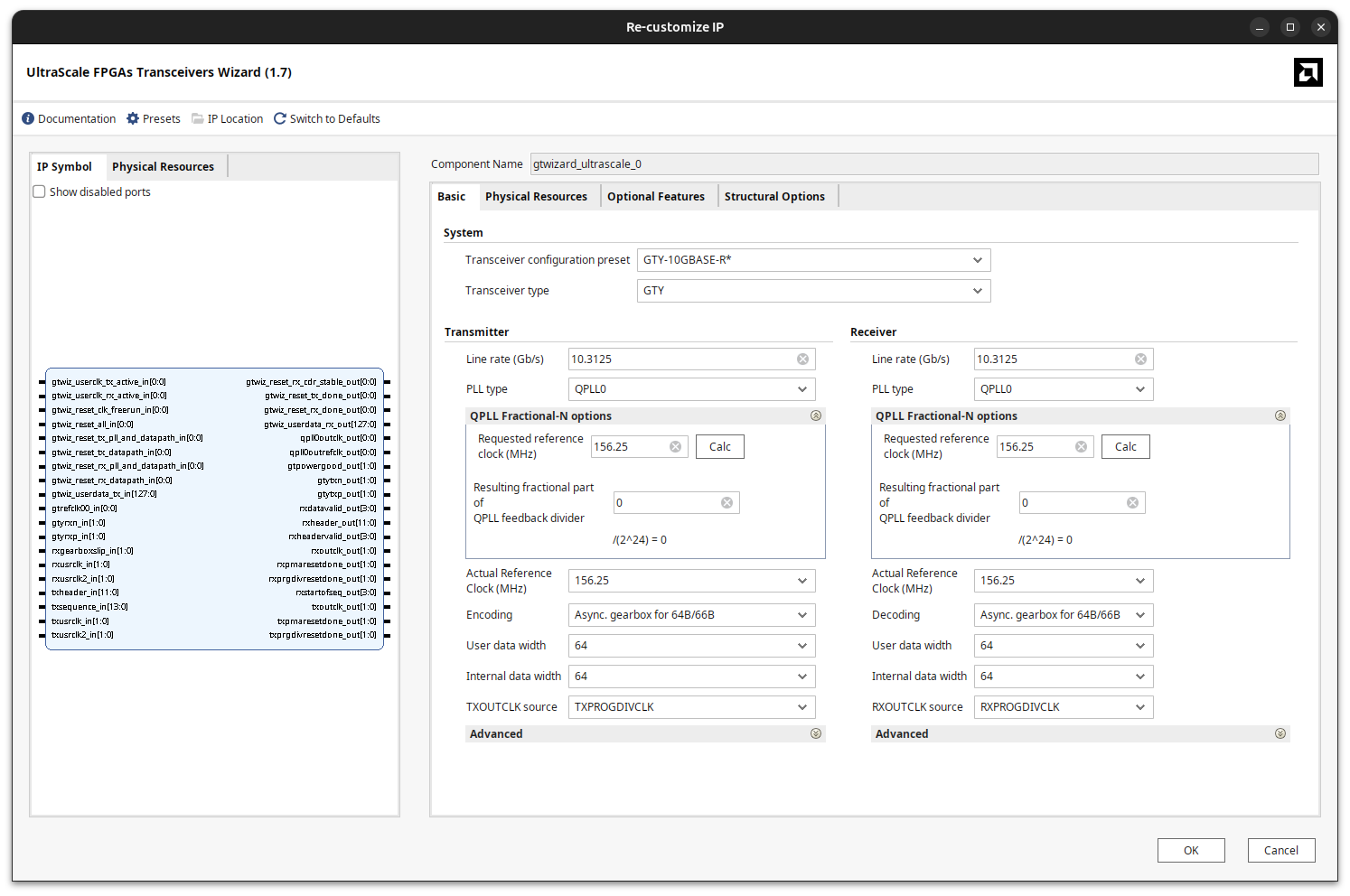
In the first tab of the wizard, we will set up a basic configuration for two GT channels. In the Transceiver Configuration Preset we will select GTY-10GBASE-R. Then, we are going to make some changes to the default configuration. The user data width is configured to 32 bits by default, but we are going to increase it to 64 bits to have a wider data path. We will make this configuration for both channels (TX and RX).
In this tab, we can see that the QPLL0 is configured for both paths, and the requested reference clock is 156.25 MHz, which matches the sfp_refclk available on the board.
Also, we can select the encoding scheme. This configuration depends on the link speed and protocol you want to use. The default value is Async. gearbox for 64B/66B. This means that, for each 64 bits of user data, the GT will add 2 bits of overhead for encoding. This is typical for 10G Ethernet links. If you are using a different protocol or speed, you may need to adjust this setting accordingly. Another widely used option is 8B/10B, but since that scheme sends 2 extra bits for every 8 bits, the effective data rate is lower.
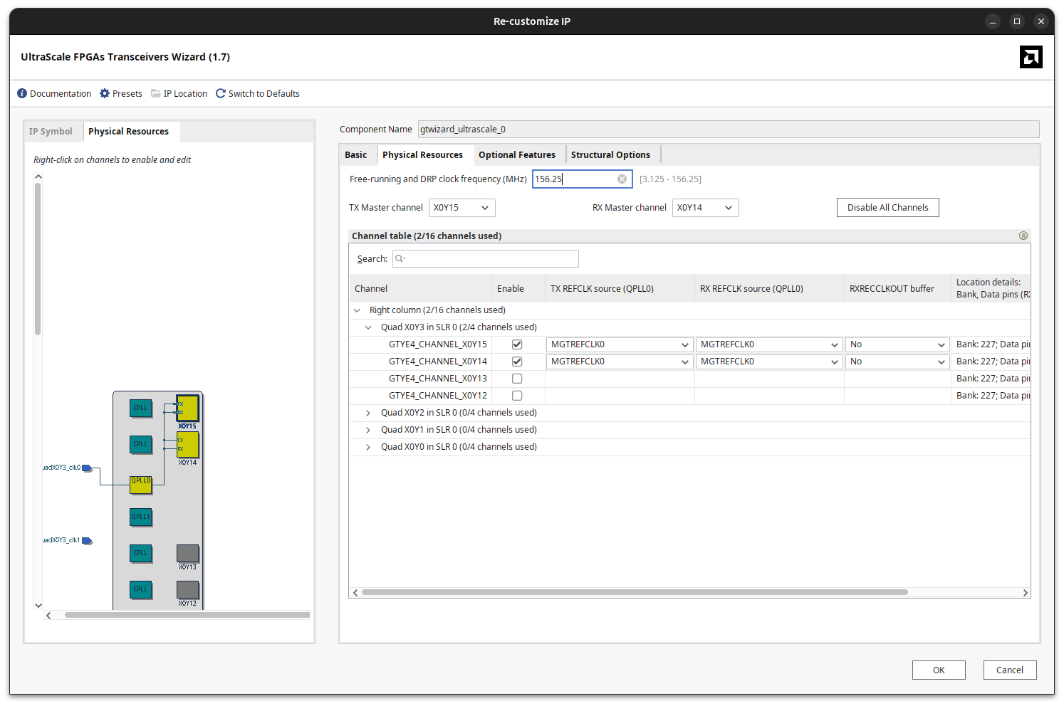
On the second tab of the wizard, we need to select the exact GTY channels that correspond to the SFP cages on the board. As I mentioned before, both SFP cages are connected to GTY Quad X0Y3, with SFP1 on channel X0Y15 and SFP2 on channel X0Y14. We can verify it by looking at the board file or the preset included in the repository.
- SFP1 → GTY channel
X0Y15(QuadX0Y3) - SFP2 → GTY channel
X0Y14(QuadX0Y3)
Regarding the reference clock, both channels share the same 156.25 MHz sfp_refclk, which is routed to the MGTREFCLK0 input of Quad X0Y3. Therefore, we can configure both channels to use a shared QPLL (QPLL0) fed by this reference clock.
With this configuration, we can generate a simple design that uses the GTY transceivers to create a loopback between SFP1 and SFP2.
Data generation and checking
To generate and check the data, we can use a simple 64-bit counter as the data source for SFP1. The counter will increment on each clock cycle, providing a known pattern of data to transmit. In addition to the payload, the Ultrascale FPGAs Transceivers Wizard allows us to send a user-defined header along with the data. This header is 6 bits per channel and can be used to identify the start of a new data frame.
Below is a very simplified version of the Verilog instantiation of the GT Wizard module, showing only the relevant signals for data transmission and reception (without including clocks and resets).
  /***************************************************************************
   * GT Wizard instantiation
   ***************************************************************************/
  gtwizard_ultrascale_0 sfp_trx_inst (
   ...
   /* 64-bit x 2 channel user data */
   .gtwiz_userdata_tx_in(gtwiz_userdata_tx_in),
   .gtwiz_userdata_rx_out(gtwiz_userdata_rx_out),
   ...
   /* GTY RX pins */
   .gtyrxn_in(gtyrxn_in),
   .gtyrxp_in(gtyrxp_in),
   ...
   /* TX header (6-bits per channel)*/
   .txheader_in(txheader_in),
   ...
   /* GTY TX pins */
   .gtytxn_out(gtytxn_out),
   .gtytxp_out(gtytxp_out),
   ...
   /* RX data valid (1 bit per channel)*/
   .rxdatavalid_out(rxdatavalid_out),
   ...
   /* RX header received (6-bits per channel) */
   .rxheader_out(rxheader_out),
   ...
   /* RX header valid (1 bit per channel) */
   .rxheadervalid_out(rxheadervalid_out),
   ...
  );
For detailed information on how to connect the GT Wizard module and handle clocks and resets, please refer to the Ultrascale FPGAs Transceivers Wizard User Guide.
On the receiver side (SFP2), we can implement a simple data checker that verifies the received data against the expected pattern. The checker will compare the received data with the expected counter value and assert an error signal if there is a mismatch.
Conclusions
I love finding hidden gems like this one, or the Kintex-7 board (also from eBay) that I talked about some time ago.
These boards are great for experimenting with large FPGAs at a very low cost, and if those FPGAs are supported by the no-cost edition of Vivado, even better. The fact that this board is designed as a PCIe NIC card makes it a bit more challenging to bring up, since there are no user interfaces or peripherals available. However, with the right resources and some reverse-engineering, it is possible to get started and experiment with the powerful GTY transceivers available on the Kintex UltraScale+ FPGA.
On the other hand, it is designed as a PCIe NIC, so there is no PMOD, no Arduino header, no buttons, and no switches—just the PCIe edge connector and the SFP cages. So, if you are looking for a development board with a bunch of peripherals, this is not the right board for you.