MicroBlaze-V on Spartan UltraScale+.
 xilinx,
microblaze,
devices,
tools,
workflow
xilinx,
microblaze,
devices,
tools,
workflow
 SCU35
SCU35
The Spartan UltraScale+ platform is currently AMD’s darling. At the FPGA events I attended this summer, the SCU35 had a special place — especially at the recent FPGA Horizons, where this board could be found not only at the AMD booth but also at AVNET’s booth.
If Spartan UltraScale+ is the favorite hardware platform, then in terms of software, the current favorite is MicroBlaze V.
MicroBlaze V is the evolution of Xilinx’s classic soft processor, redesigned around the RISC-V architecture and intended for integration into the latest AMD platforms. It preserves the hallmark flexibility of MicroBlaze — a fully synthesizable CPU within the FPGA fabric — while adopting the 32-bit RISC-V instruction set, allowing it to benefit from a much broader ecosystem of open-source compilers, debuggers, and development tools.
Does this mean the classic MicroBlaze is over? Personally, I think that in the near future it won’t be officially supported by AMD, and that in a later version of Vivado it will be completely replaced by MicroBlaze V.
In this article, we are going to deploy a MicroBlaze V soft core on the SCU35 board, and in the final step, we are going to add an ILA to the hardware design in order to debug the AXI interfaces.
Table of Contents
- Project Setup in Vivado
- Build the SoC in IP Integrator
- Clocking, Reset, and Memory Map
- Generate Bitstream & Export XSA
- Create the Application in Vitis
- Debugging AXI4 Lite with ILA
Project Setup in Vivado
The first step is creating the project in Vivado. Usually we are going to do this using the graphical interface, but if we are working with the project in a repository, we would like to reduce as much as possible the size of the files we will upload, so in this case we can upload the script to regenerate the project instead of the project itself.
The next script creates a project for the SCU35 board in the proj_dir directory with the name proj_name.
################################################################################
# TCL script to regenerate Vivado project from block design TCL
# Targeting SCU35 FPGA board
# Vivado version: 2025.1
# Author: PTrujillo
# Date: 2025-08-31
################################################################################

####### Set project variables
set proj_name "scu35_microblaze"
set proj_dir "../../project"

####### Create project
create_project $proj_name $proj_dir -force

####### Set the board part (SCU35)
set_property board_part xilinx.com:scu35:part0:1.0 [current_project]
If we have the tcl of the block design, we can also include the generation of the block design by adding source $bd_tcl_code, where bd_tcl_code is the file containing the tcl code for the block design.
Since it is not our case, once the project is created we can open it from Vivado, create a new block design, and start working with it.
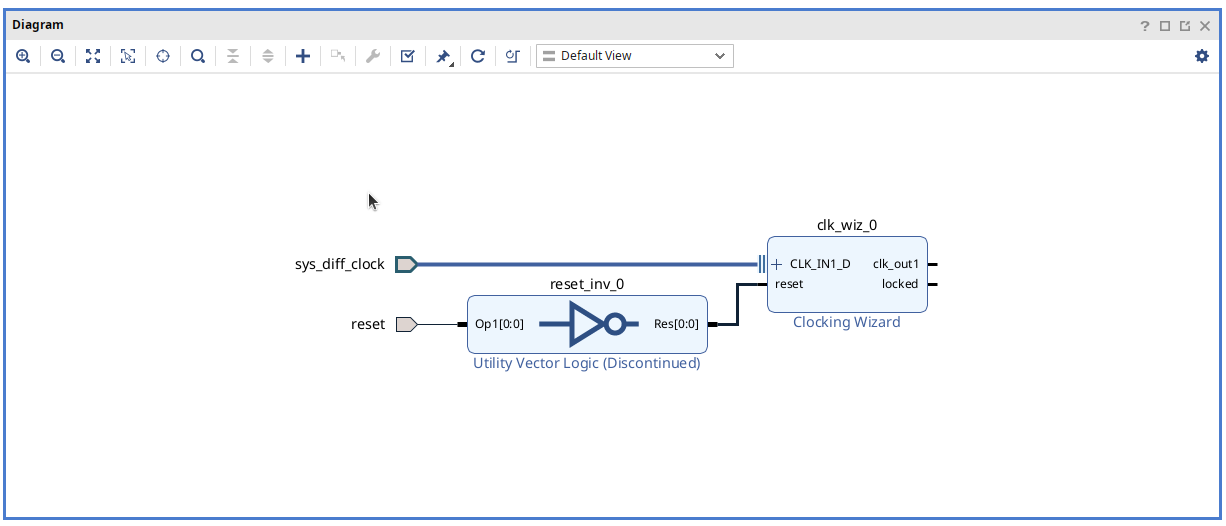
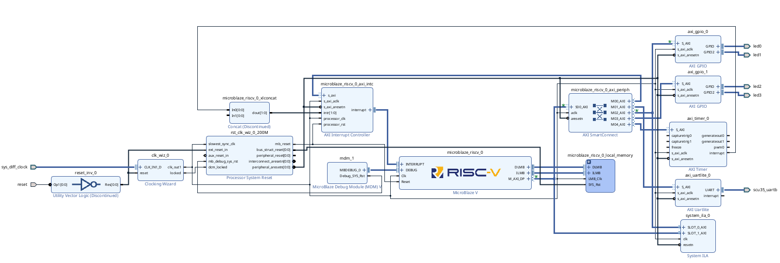
Clocking and Reset
The first block we are going to add is the clock from the Boards components. When the clock is added to the block design, we are going to increase the frequency to 200 MHz.

Now, by clicking on Run Connection Automation, we are going to include the negated reset. If you do this by adding the reset from the Board componentes, the reset inluded will be a non.negated reset, witch is not valid for this design.
Build the SoC in IP Integrator
Next, we are going to include in the block design the rest of the components. For this example, we are going to include in first place the Microblaze-V soft core.

By clocking on Run Block Automation, we will be able of customizing some elements of the soft-core like the preset, the amount of memory attached. whether we want to add the debug module or not, the AXi peripherals port inclusion and the interrupt controller.

For more customization options, like the especific type of risc-v core used, we can open the block properties in the block design.
Now, we can add the rest of the blocks of the design. For this project we will need to include from the Board components AXI uart Lite, and the LED which will add two AXI GPIO blocks. Then we will add from the IP catalog an AXI Timer.

The AXI Timer IP is optional, but it ensures that when using the delay.h library in the application, the timing will be more accurate.
If we do not include the AXI Timer IP, the delay functions will still work, but they will generate delays using software loops, meaning that the exact duration will depend on the rest of the application.
Memory Map
When all the blocks are added to the block design, we canverify the design and check the memory map of the design.
From this memory map, we can increase or decrease the amount of memory dedicated to the Microblaze-V soft core by modifying the *_local_memory nodes.
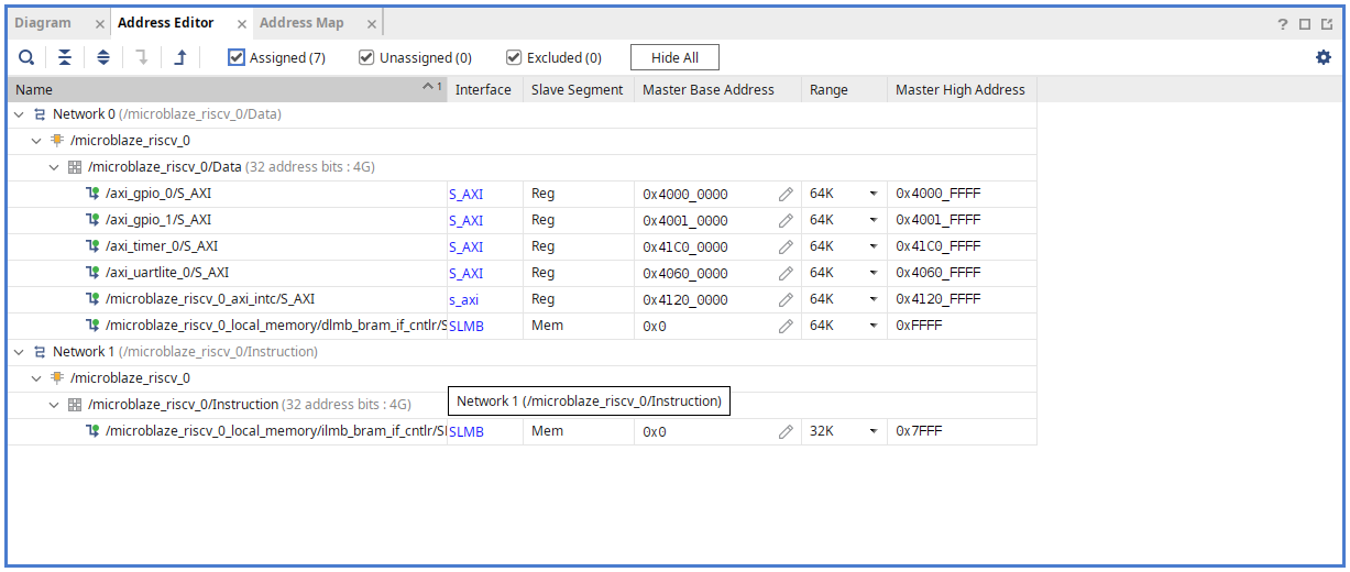
Notice that there are two lmp memories, one for instructions, and the other one for data, although later will be the linker the one in charge of select which memory will store data and instructions.
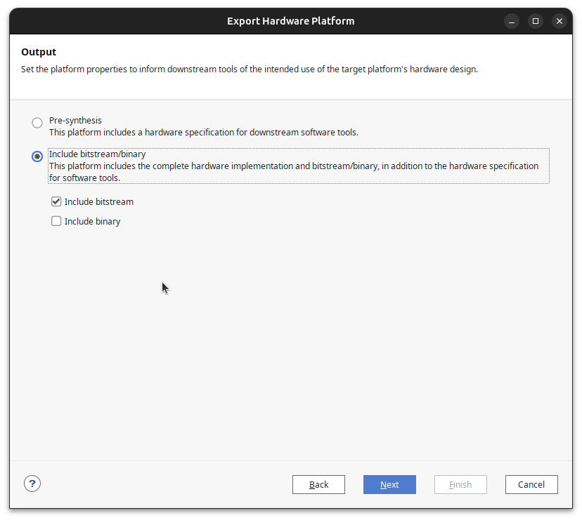
Generate Bitstream & Export XSA
Now, we have the block design complete and, as always, we have to create the wrapper of the block design, that will create a Verilog code from the block design and finally generate the device image.
When the image is created, there’s only one step left in Vivado, which is export the hardware. This step will generate the .xsa file that contains all the needed files by Vitis.
Create the Platform in Vitis
The next steps will be executed from Vitis, so we can open Vitis from the command line or navigate in VIvado to Flow > Launch Vitis.
On Vitis, the first step is to create the HW platform in which we are goping to execute the applications.
Once we have a workspace selected, we just need to click on Create Platform Component, and follow the steps to create the platform.

remember that the platform is a project itself, so we need to build it.
Create the Application in Vitis
When we have the platform ccreated and built, now we are ready for creating applications to run into. We can start by an example, o creating an empty project, and then create the different source files.
In order to test that everything is ready, we can create a basic application that uses the UART to send an string.
/**
 * @file main_hello_world.c
 * @brief Hello World application for Microblaze AXI_UART
 *
 * This application prints "Hello world from the SCU35!" to the UART terminal.
 * It is intended to run on a Microblaze soft core with AXI_UART configured.
 *
 * UART output is handled by the standard printf function, which uses the BSP's
 * low-level drivers to send data over the AXI_UART peripheral.
 *
 * @author PTrujillo
 * @date 09/2025
 */

#include <stdio.h>

/**
 * @brief Main entry point
 *
 * Prints a hello world message over UART and loops forever.
 */
int main() {
    printf("Hello workd from the SCU35!\r\n");
    while (1) {
        // Loop forever
    }
    return 0;
}
When the application is created, the next step is needed at least for me, let me explain. The theoretical next step is debug the application. By doing this, Vitis will, in first place, load the bitstream on to FPGA, and then load the memory content with the application. In my case, the FPGA is configured, but the load of the application fails because it does not find an ARM core, which is correct.
In order to make it work, I need to, first, load the bitstream from Vivado, and then, uncheck the option Program Device in the launch.json file of the project.
This configuration makes that the Vitis application only loads the application, and since the soft-core is already configured, everything works well.
For this application, we need to open the created COM port fromk the host computer, and check that the string is send correctly.
Another example that uses the AXI GPIO to manage the RGB leds is the next.
/**
 * @file main_led_control.c
 * @brief LED control application for Microblaze-V AXI_UART and AXI_GPIO
 *
 * - AXI_GPIO0 base address: 0x40000000 (LEDs 1 & 2)
 * - AXI_GPIO1 base address: 0x40010000 (LEDs 3 & 4)
 *
 * @author PTrujillo
 * @date 09/2025
 */

#include "xil_io.h"
#include "sleep.h"

/* GPIO Base Address */
#define AXI_GPIO_BASE_ADDRESS 0x40000000

/* AXI GPIO registers */
#define GPIO_DATA_OFFSET   0x0
#define GPIO_TRI_OFFSET    0x4

int main (void) {

    int led_counter;

    /* Init GPIO */
    Xil_Out32(AXI_GPIO_BASE_ADDRESS+GPIO_TRI_OFFSET, 0x0); // all outputs
    Xil_Out32(AXI_GPIO_BASE_ADDRESS+GPIO_DATA_OFFSET, 0x0); // leds off

    led_counter = 0;

    while(1){
        if (led_counter == 3)
            led_counter = 0;
        else
            led_counter++;

        Xil_Out32(AXI_GPIO_BASE_ADDRESS+GPIO_DATA_OFFSET, led_counter);

        sleep(1);
    }

    return 1;
}
Debugging AXI4 Lite with ILA
Now, we are going to debug the AXI bus
To add the ILA, we just need to select the line, and doind right click select the option Debug. This will activate the banner Run Connection Automation, and by clicking on it the ILA configuration will be opened.
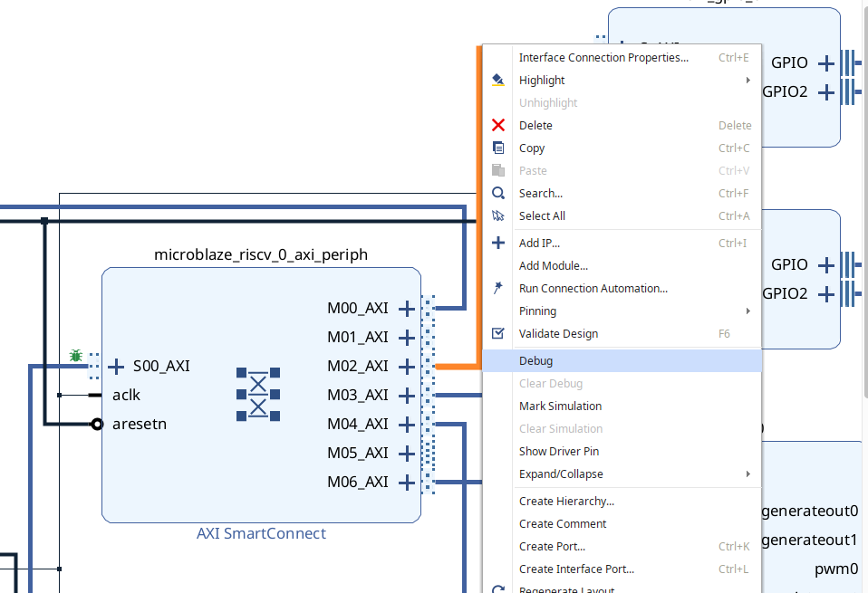
Once the configuration is finished, the IP System ILA will be added to the design.
Now, we can generate the Device Image, and finally load it into the FPGA. Also, the .ltx file with the information of the probes will be added.
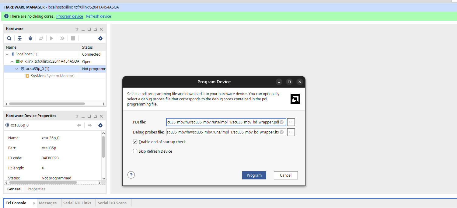
When the FPGA is configured, automatically the Waveform view will be opened. Then, we can load the application from Vitis, and debug it.
To capture the AXi transactions, notice that AXI channels have two different channels, one for the address sending, and the otherone for the data sending. If we want to capture the antire AXi transaction, we can start capturing when the address is sent, so we can configure the trigger in the address data valid signal AWVALID.
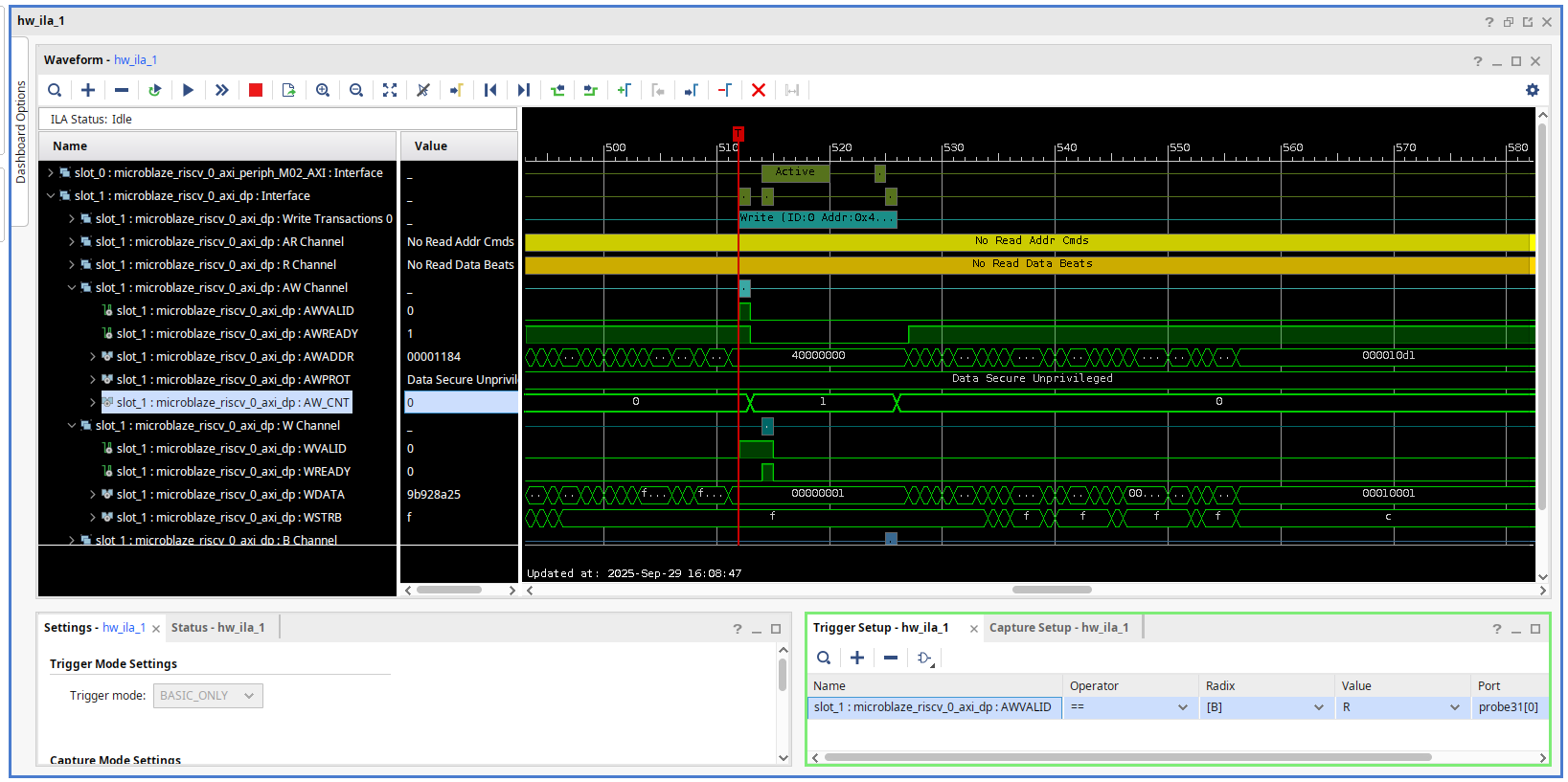
Now we can run the application, and the first AXI transactions will be captured by the ILA cores.
I wrote an article a year ago where I asked whether a platform like AMD Spartan UltraScale+ makes sense, and today I have to say that it is filling a gap between regular FPGAs and some features — especially those related to security — from Zynq UltraScale+ and even Versal. Actually, I’m now wondering whether Artix UltraScale+ makes sense, except for the GTH transceivers in the smaller devices.
In any case, I can’t wait to see new Spartan UltraScale+ boards, especially one with DDR5 to be able to add a TCP/IP stack to the soft core.